The hardware platform for this article is: ZC702 (XC7Z020-1CLG484CES). The software used includes: PlanAhead, Xilinx Platform Studio, and Xilinx Software Development Kit, all of which are 14.4. The serial port tool is Tera Term.
The ZYNQ-7000 is a fully programmable system-on-chip (I/O) from Xilinx that integrates the ARM Cortex A9 dual-core and FPGA, so ZYNQ is a SoPC chip. Its architecture is as follows:
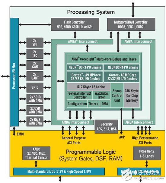
The Processing System (commonly referred to as PS) in the figure is the processor (ARM Cortex A9 MPCore) part, which is very rich in resources. For details, please refer to the official Xilinx documentation. Programmable Logic (commonly referred to as PL) can be programmed (FPGA), the resources of this part vary with SoC chip level, the lowest is ArTIx-7 (Zynq-7010 and Zynq-7020), the highest is Kintex- 7 (Zynq-7030 and Zynq-7045). Of course, it is unclear that subsequent FPGAs in the SoC will use the higher Virtex series.
The relationship between PS and PL:The essence of PS is an ARM Cortex A9 MPcore, so if we don't use the programmable part, we can just use the PS part. That is to say, for the ZYNQ chip, the PS part can be used completely independently, independent of the PL part.
The essence of the PL part is the Xilinx FPGA. In ZYNQ, we can think of PL as another "peripheral" of PS that has reconfigurable features. It can be used as a slave of the PS part and controlled by the ARM processor. For example, if the number of serial ports of the ARM (PS) is not enough, the PL interface can be extended when the Ethernet interface is not enough, or when the video interface is required. Of course, we can also regard the PL part as a master device that is not controlled by the ARM processor and is equivalent to the ARM processor, and actively performs data interaction with external chips and interfaces. Even the PL part can be used as the master device of the whole system, actively acquiring and storing data from the memory of the APU part, and controlling the operation of the ARM processor. Therefore, in theory, the PL part can also operate independently like the PS part. But the limitation is that the PL part must be configured using the JTAG interface. If there is no JTAG interface, it cannot run independently, because both the PS part and the PL part of ZYNQ must rely on PS to complete the initial configuration of the chip.
As embedded systems become more complex and more powerful, they often require very flexible FPGAs in the design, as well as processors to do some control and use with the operating system. The traditional approach is to use an FPGA chip and a processor chip, such as FPGA + ARM mode. However, in this mode, communication between FPGA and ARM is often the bottleneck of the system. However, in ZYNQ7000, the FPGA and ARM are integrated in one chip, and the communication between the two uses AXI_HP, AXI_GP, AXI_ACP three kinds of interfaces to communicate, the bandwidth can reach gigabit, basically there is no problem of insufficient communication bandwidth between the two. . Of course, there is also a traditional implementation of a soft core on the FPGA (such as Altera's Nios II, Xilinx's Picoblaze, Micoblaze, etc.), which is sufficient for some applications where the processor is not demanding, but if the processor requirements are compared High scenes, the performance of this soft core is often stretched. And the soft core will take up some of the PFGA resources. Therefore, the ZYNQ series realizes the integration of FPGA and hard core, which is a milestone for embedded development design.
Xilinx provides three main software developments for ZYNQ: PlanAhead, Xilinx Platform Studio (XPS), and Xilinx Software Development Kit (SDK). Of course, the positioning and function of these three softwares, Xilinx and the Internet have very detailed and very official instructions, I will not go into details. I personally understand that PlanAhead is to build the entire hardware environment and integrate the system. XPS can be called directly from PlanAhead, mainly for the development and design of the processor part. The SDK is Xilinx's modification of Eclipse, mainly used for the design of the software part. Of course, Xilinx has launched a new generation of design software Vivado, which can be found on the Xilinx website.
Of course, the design and structure of the ZYNQ series of chips itself is very complicated, and the technology involved is much more, because the positioning of this series of articles will not summarize these. And it's not necessary. These things can be found in the documentation provided by Xilinx. I will only summarize some things that are not mentioned in the documentation, or that are not summarized in the system.
Yoga Laptop,2-In-1 Yoga Laptop,Quad-Core Notebook,Notebook Computer Office
C&Q Technology (Guangzhou) Co.,Ltd. , https://www.gzcqteq.com