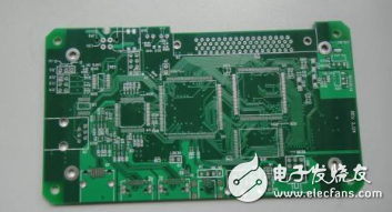
Speaking of PCB, many friends will think that it can be seen everywhere around us. From all household appliances, various accessories in computers, to various digital products, as long as electronic products almost always use PCB, then what is PCB? The PCB is the PrintedCircuitBlock, which is a printed circuit board that is placed for electronic components and has a line base. The copper plated substrate is printed with an anti-corrosion line by printing and etched out of the line.
PCBs can be divided into single-layer boards, double-layer boards, and multi-layer boards. Various electronic components are integrated on the PCB. On the most basic single-layer PCB, the parts are concentrated on one side, and the wires are concentrated on the other side. In this case, we need to make holes in the board so that the pins can pass through the board to the other side, so the parts are soldered to the other side. Because of this, the front and back sides of such a PCB are called ComponentSide and SolderSide, respectively. The double-layer board can be seen as consisting of two single-layer boards that are relatively bonded together, with electronic components and traces on both sides of the board. Sometimes it is necessary to connect a single wire on one side to the other side of the board, which is through the via. The via hole is a small hole filled or coated with metal on the PCB, which can be connected to the wires on both sides. Many computer motherboards now use 4 or even 6-layer PCBs, and graphics cards generally use 6-layer PCBs. Many high-end graphics cards use 8-layer PCBs like the nVIDIA GeForce4Ti series. This is called multi-layer PCB.
The problem of connecting the lines between the layers is also encountered on the multilayer PCB, and can also be achieved through the via holes. Because of the multi-layer PCB, sometimes the vias do not need to penetrate the entire PCB. Such vias are called Buriedvias and Blindvias because they only penetrate several layers. A blind hole connects several layers of internal PCB to a surface PCB without penetrating the entire board. The buried hole is only connected to the internal PCB, so the light is not visible from the surface. In the multi-layer PCB, the entire layer is directly connected to the ground wire and the power supply. So we classify each layer as a signal layer, a power layer or a ground layer. If the parts on the PCB require different power supplies, this type of PCB typically has more than two layers of power and wiring. The more PCB layers are used, the higher the cost. Of course, using more layers of PCB is very helpful in providing signal stability. The professional PCB manufacturing process is quite complicated, taking a 4-layer PCB as an example.
The motherboard's PCB is mostly 4 layers. When manufacturing, the middle two layers are respectively crushed, cut, etched, oxidized and electroplated. The four layers are the component surface, the power layer, the ground layer and the solder layer. Then put these 4 layers together and crush them into a PCB of a motherboard. Then punch holes and make holes. After washing, the outer two layers of the line are printed, copper coated, etched, tested, solder mask, silk screen. Finally, the whole PCB (including many motherboards) is stamped into the PCB of the motherboard, and then vacuum-packed after passing the test. If the copper coating is not well applied during the PCB manufacturing process, the paste may not be firmly adhered, and it is easy to imply a short circuit or a capacitive effect (prone to interference). Vias on the PCB must also be noted. If the hole is not in the middle, but is biased to the side, it will produce a non-uniform match, or it will easily come into contact with the middle power layer or the ground layer, resulting in potential short circuit or poor grounding.
Copper wiring process
The first step in the production is to create wiring that connects the parts. We use a negative transfer method to present the working film on a metal conductor. The trick is to lay a thin layer of copper on the entire surface and remove the excess. Additional transfer is another way of using less people. This is a way to apply copper wire only where needed, but we won't talk much about it here. A positive photoresist is made of a sensitizer that dissolves under illumination. There are many ways to handle photoresist on copper surfaces, but the most common way is to heat it and roll it on the surface containing the photoresist. It can also be sprayed on the head in a liquid state, but the dry film type provides a higher resolution and can also make a thinner wire. The hood is just a template for the PCB layer in the manufacturing process. Before the photoresist on the PCB is exposed to UV light, the hood overlying it prevents some areas of the photoresist from being exposed. These places covered by photoresist will become wiring. Other bare copper portions to be etched after development of the photoresist. The etching process can immerse the board in an etching solvent or spray the solvent onto the board. Generally used as an etching solvent, ferric chloride or the like is used. The remaining photoresist is removed after the etching is completed.
1. Wiring width and current
Generally, the width should not be less than 0.2mm (8mil) on a high-density and high-precision PCB. The pitch and line width are generally 0.3mm (12mil). When the thickness of the copper foil is about 50um, the width of the wire is 1~1.5mm (60mil) = 2A is generally 80mil, which is more important for applications with microprocessors.
2. How high is the high speed board?
When the rising/falling edge time of the signal is < 3~6 times of the signal transmission time, it is considered as a high-speed signal. For digital circuits, the key is to look at the steepness of the edge of the signal, that is, the rise and fall time of the signal, according to a very classic According to the book "High Speed ​​Digtal Design", the signal rises from 10% to 90% less than 6 times the wire delay, which is the high-speed signal!------ That is, even if the 8KHz square wave signal, as long as the edge is enough Steep, the same high-speed signal, the use of transmission line theory in wiring
3. PCB stacking and layering
In order to have a better electromagnetic compatibility design, the multilayer printed board can meet the electromagnetic compatibility and sensitivity standards during normal operation. Proper stacking helps shield and suppress EMI. The following basic principles are generally followed in delamination and stacking of multilayer printed boards:
1 The power plane should be as close as possible to the ground plane and should be below the ground plane.
2 The wiring layer should be arranged adjacent to the image plane layer.
3 Power and formation impedance are lowest.
4 A strip line is formed in the middle layer, and a microstrip line is formed on the surface. The characteristics of the two are different.
5 Important signal lines should be close to the ground.
A very important advantage of multi-layer boards over ordinary double-layer boards and single-layer boards is that signal lines and power supplies can be distributed on different board layers to improve signal isolation and anti-interference performance. However, many engineers still have headaches about PCB delamination and stacking, taking the commonly used 4-layer board as an example. The four-layer board has the following stacking sequences. The following explains the advantages and disadvantages of various stacks:
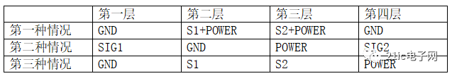
Note: S1 signal wiring layer, S2 signal wiring layer 2; GND ground layer POWER power layer in the first case, should be the best case of the four-layer board. Because the outer layer is the ground layer, it has a shielding effect on EMI, and the power layer is also reliable close to the ground layer, so that the internal resistance of the power source is small, and the best suburban fruit is obtained. However, the first case cannot be used when the density of the board is relatively large. Because of this, the integrity of the first layer cannot be guaranteed, and the second layer signal will become worse. In addition, this structure cannot be used in the case where the power consumption of the whole board is relatively large. The second case is one of the most common ways we usually use. From the structure of the board, it is not suitable for high-speed digital circuit design. Because in this configuration, it is difficult to maintain a low power supply impedance. Take a plate of 2 mm as an example: Z0 = 50 ohms is required. The line width is 8 mils. The thickness of the copper foil is 35 цm. Thus the middle of the signal layer is 0.14mm between the ground and the ground. The formation and power layer are 1.58mm. This greatly increases the internal resistance of the power supply. In this structure, since the radiation is spatial, a shield plate is required to reduce EMI. In the third case, the signal quality on the S1 layer is the best. S2 is second. It has a shielding effect on EMI. However, the power supply impedance is large. This board can be used when the power consumption of the whole board is large and the board is the source of interference or close to the source of interference.
4. Impedance matching
The amplitude of the reflected voltage signal is determined by the source reflection coefficient Ïs and the load reflection coefficient ÏL ÏL = (RL - Z0) / (RL + Z0) and ÏS = (RS - Z0) / (RS + Z0) in the above equation, If RL = Z0, the load reflection coefficient ÏL = 0. If RS = Z0 source reflection coefficient ÏS = 0. Since the ordinary transmission line impedance Z0 should normally satisfy the 50 Ω requirement of about 50 Ω, the load impedance is usually in the range of several thousand ohms to several tens of kilo ohms. Therefore, it is difficult to achieve impedance matching on the load side. However, since the signal source (output) impedance is usually small, it is roughly a dozen ohms. Therefore, it is much easier to achieve impedance matching at the source. If the resistor is connected in parallel with the load, the resistor will absorb some of the signal and it will be unfavorable for transmission (I understand). When the TTL/CMOS standard 24mA drive current is selected, its output impedance is approximately 13Ω. If the transmission line impedance Z0 = 50Ω, then a 33Ω source termination resistor should be added. 13Ω+33Ω=46Ω (approximately 50Ω, weak underdamping contributes to the setup time of the signal). When other transmission standards and drive currents are selected, the matching impedance will vary. In high-speed logic and circuit design, for some key signals, such as clocks, control signals, etc., we recommend that you must add source-side matching resistors. In this way, the signal is also reflected back from the load end. Because the source impedance matches, the reflected signal will not be reflected back.
5. Power cord and ground wire layout precautions
The Power Cable is as short as possible, straight, and it is best to go tree-shaped, do not take the loop ground loop problem: For digital circuits, the ground loop caused by the ground loop is tens of millivolts, and TTL The anti-interference threshold is 1.2V, and the CMOS circuit can reach 1/2 power supply voltage, which means that the ground loop will not adversely affect the operation of the circuit. On the contrary, if the ground wire is not closed, the problem will be even bigger, because the pulse power supply current generated by the digital circuit will cause the ground potential imbalance at each point. For example, I measured the ground current of the 74LS161 in reverse when the inverter is 1.2A. The 2Gsps oscilloscope measured the ground current pulse width of 7ns). Under the impact of large pulse current, if a distributed ground line (line width 25 mil) is used, the potential difference between the ground lines will reach the level of 100 millivolts. After the ground loop is used, the pulse current is spread to various points of the ground line, which greatly reduces the possibility of interference with the circuit. With the closed ground wire, the maximum instantaneous potential difference of the ground of each device is measured to be one-half to one-fifth of the unclosed ground. Of course, the measured data of boards with different densities and different speeds are very different. I said above, it refers to the level of the Z80 Demo board attached to the Protel 99SE. For the low-frequency analog circuit, I think the power frequency after the ground line is closed. Interference is sensed from space, which is not simulated or calculated anyway. If the ground wire is not closed, there will be no ground eddy current. Beckhamtao said, "But the ground-frequency open loop, the power frequency induced voltage will be larger." The theoretical basis and the two examples, I took over one of the others 7 years ago. The project, precision pressure gauge, uses a 14-bit A/D converter, but the actual measurement has only 11 effective precision. After investigation, there is 15mVp-p power frequency interference on the ground. The solution is to simulate the ground loop of the PCB. Scratch, the front-end sensor to the A/D ground wire is distributed by the flying line. Later, the mass-produced model PCB is again produced according to the flying line, and there has been no problem so far. The second example, a friend loves a fever, DIY a power amplifier, but the output always has a hum, I suggest it cut the ground loop, the problem is solved. Afterwards, this man looked at dozens of "Hi-Fi machine" PCB diagrams, confirming that no machine used a ground loop in the analog part.
6. Printed circuit board design principles and anti-interference measures
A printed circuit board (PCB) is a support for circuit components and devices in an electronic product. It provides an electrical connection between the circuit components and the device. With the rapid development of electricity technology, the density of PGB is getting higher and higher. The quality of PCB design has a great influence on the interference capability. Therefore, in the PCB design, the general principles of PCB design must be observed and the requirements of anti-interference design should be met. The general principle of PCB design is to achieve the best performance of the electronic circuit, the layout of the components and the layout of the wires is very important. In order to design a good quality, low cost PCB. The following general principles should be followed: layout First, consider the PCB size. When the PCB size is too large, the printed lines are long, the impedance is increased, the anti-noise ability is lowered, and the cost is also increased; if the size is too small, the heat dissipation is not good, and adjacent lines are susceptible to interference. After determining the PCB size, determine the location of the special component. Finally, according to the functional unit of the circuit, all the components of the circuit are laid out.
Observe the following principles when determining the location of a particular component:
(1) Try to shorten the wiring between high-frequency components as much as possible, and try to reduce their distribution parameters and mutual electromagnetic interference. Components that are susceptible to interference cannot be placed too close together, and input and output components should be kept as far away as possible.
(2) There may be a high potential difference between some components or wires, and the distance between them should be increased to avoid accidental short circuit caused by discharge. Components with high voltage should be placed as far as possible in the hands of the hand when debugging.
(3) Components weighing more than 15g shall be fixed by brackets and then welded. Those components that are large, heavy, and have a lot of heat should not be mounted on the printed board, but should be installed on the chassis of the whole machine, and heat dissipation should be considered. The thermal element should be kept away from the heating element.
(4) For the layout of adjustable components such as potentiometers, adjustable inductors, variable capacitors, microswitches, etc., the structural requirements of the whole machine should be considered. If it is adjusted inside the machine, it should be placed on the printed board to facilitate adjustment; if it is adjusted outside the machine, its position should be compatible with the position of the adjustment knob on the chassis panel.
(5) The position occupied by the printing plate positioning hole and the fixing bracket should be left.
According to the functional unit of the circuit. When laying out all the components of the circuit, the following principles must be met:
(1) Arrange the position of each functional circuit unit according to the flow of the circuit, so that the layout facilitates signal circulation and keeps the signal as consistent as possible.
(2) Center around the core components of each functional circuit and arrange it around it. Components should be evenly, neatly and compactly placed on the PCB. Minimize and reduce leads and connections between components.
(3) For circuits operating at high frequencies, the distribution parameters between components should be considered. In general, the circuit should be arranged in parallel as much as possible. In this way, it is not only beautiful, but also easy to load and weld. It is easy to mass produce.
(4) The components located at the edge of the board are generally not less than 2 mm from the edge of the board. The optimal shape of the board is a rectangle. The aspect ratio is 3:2 to 4:3. When the board surface size is larger than 200x150mm, the mechanical strength of the board should be considered.
2. The principle of wiring and wiring is as follows:
(1) The wires used at the input and output terminals should be avoided as far as possible. It is best to add the ground wire between the wires to avoid feedback.
(2) The minimum width of the printed photoconductive wire is mainly determined by the adhesion strength between the wire and the insulating base plate and the current value flowing through them. When the thickness of the copper foil is 0.05mm and the width is 1 ~ 15mm, the temperature will not exceed 3 °C through the current of 2A. Therefore, the wire width of 1.5mm can meet the requirements. For integrated circuits, especially digital circuits, a wire width of 0.02 to 0.3 mm is usually selected. Of course, as far as possible, use wide lines as much as possible, especially power and ground. The minimum spacing of the wires is primarily determined by the worst case interline insulation resistance and breakdown voltage. For integrated circuits, especially digital circuits, the pitch can be as small as 5~8mm as long as the process allows.
(3) The curved corner of the printed conductor generally takes a circular arc shape, and the right angle or angle affects the electrical performance in the high frequency circuit. In addition, try to avoid the use of large areas of copper foil, otherwise, when heated for a long time, copper foil expansion and shedding are prone to occur. When a large area of ​​copper foil is used, it is preferable to use a grid shape. This is advantageous in eliminating the volatile gas generated by the heat of the adhesive between the copper foil and the substrate. 3. The pad pad center hole is slightly larger than the device lead diameter. The pad is too large to form a solder joint. The pad outer diameter D is generally not less than (d + 1.2) mm, where d is the lead aperture. For high-density digital circuits, the minimum pad diameter can be (d + 1.0) mm.
PCB and circuit anti-interference measures The anti-interference design of the printed circuit board has a close relationship with the specific circuit. Here, only some common measures of PCB anti-interference design are explained.
1. Power line design According to the current of the printed circuit board, try to increase the width of the power line and reduce the loop resistance. At the same time, the direction of the power line and the ground line is consistent with the direction of data transmission, which helps to enhance the anti-noise capability.
2. Ground wire design The principle of ground wire design is: (1) The digital ground is separated from the simulated ground. If there are both logic and linear circuits on the board, they should be separated as much as possible. The ground of the low-frequency circuit should be grounded in parallel with a single point. If the actual wiring is difficult, it can be partially connected and then grounded in parallel. The high-frequency circuit should adopt multi-point series grounding, the ground wire should be short and rented, and the grid-like large-area foil should be used as much as possible around the high-frequency components. (2) The grounding wire should be as thick as possible. If the grounding wire uses a very strong line, the grounding potential changes with the change of the current, which reduces the noise immunity. Therefore, the ground wire should be thickened so that it can pass three times the allowable current on the printed board. If possible, the grounding wire should be 2~3mm or more. (3) The grounding wire constitutes a closed loop. In a printed circuit board composed only of digital circuits, the grounding circuit is mostly formed into a loop, which can improve the anti-noise capability.
3. One of the common practices of PCB design for unpacking capacitors is to configure appropriate untwisting capacitors at each critical part of the board. The general configuration principle of the untwisting capacitor is: (1) The power input terminal is connected to an electrolytic capacitor of 10 ~ 100 uf. If possible, it is better to pick up 100uF or more. (2) In principle, each integrated circuit chip should be equipped with a 0.01pF ceramic capacitor. If there is insufficient gap in the printed board, a capacitor of 1 ~ 10pF can be arranged every 4~8 chips. (3) For devices with weak anti-noise capability and large power supply changes during shutdown, such as RAM and ROM storage devices, the decoupling capacitor should be directly connected between the power cable and the ground of the chip. (4) The capacitor leads should not be too long, especially the high-frequency bypass capacitors must not have leads. In addition, you should also pay attention to the following two points: (1) When there are contactors, relays, buttons and other components in the printed board, a large spark discharge will occur when operating them, and must be absorbed by the RC circuit shown in the figure. Discharge current. Generally, R takes 1 ~ 2K and C takes 2.2 ~ 47UF. (2) The input impedance of CMOS is very high and it is susceptible to induction. Therefore, it is necessary to ground or connect the power supply to the unused terminal during use.
7. Design tips and key points for efficient PCB automatic routing
Although the current EDA tools are very powerful, as PCB size requirements become smaller and the device density becomes higher and higher, PCB design is not difficult. How to achieve high PCB layout and shorten design time? This article introduces the design skills and key points of PCB planning, layout and wiring. PCB design time is getting shorter and shorter, smaller and smaller board space, higher device density, extremely harsh layout rules and large size components make the designer's work more difficult. In order to solve the design difficulties and speed up the market launch, many manufacturers now prefer to use dedicated EDA tools to achieve PCB design. However, dedicated EDA tools do not produce the desired results, nor can they achieve 100% throughput, and they are messy, and usually take a lot of time to complete the rest of the work. There are a lot of EDA tools available on the market, but they are similar except that the terms and function keys are different. How to use these tools to better design the PCB? Carefully analyze the design before starting the wiring and Careful setup of the tool software will make the design more compliant. Below are the general design procedures and procedures.
1, determine the number of layers of the PCB
Board size and number of wiring layers need to be determined early in the design process. If the design requires the use of high-density ball grid array (BGA) components, the minimum number of routing layers required for wiring these devices must be considered. The number of wiring layers and the stack-up method directly affect the wiring and impedance of the printed wiring. The size of the board helps determine the stacking and line width to achieve the desired design. For many years, people have always thought that the lower the number of board layers, the lower the cost, but there are many other factors that affect the manufacturing cost of the board. In recent years, the cost difference between multilayer boards has been greatly reduced. At the beginning of the design, it is better to use more circuit layers and evenly distribute the copper to avoid a small number of signals that do not meet the defined rules and space requirements at the end of the design, and thus be forced to add new layers. Careful planning before design will reduce a lot of trouble in wiring.
2, design rules and restrictions
The autorouting tool itself does not know what to do. To complete the routing task, the routing tool needs to work under the correct rules and constraints. Different signal lines have different wiring requirements, and all special required signal lines are classified, and different design classifications are also different. Each signal class should have priority. The higher the priority, the stricter the rules. The rules relate to the width of the trace, the maximum number of vias, the parallelism, the interaction between the signal lines, and the limitations of the layers, which have a large impact on the performance of the routing tool. Careful consideration of design requirements is an important step in successful cabling.
3, the layout of the components
To optimize the assembly process, the Manufacturability Design (DFM) rules place restrictions on the component layout. If the assembly department allows the components to move, the circuit can be properly optimized for easier automatic routing. The defined rules and constraints affect the layout design. The routing channel and via area should be considered when laying out. These paths and areas are obvious to the designer, but the automatic routing tool only considers one signal at a time. By setting the wiring constraints and setting the layers of the signal lines, the routing tools can be imagined by the designer. That completes the wiring.
4, fanout design
In the fan-out design phase, for the auto-wiring tool to connect the component pins, each pin of the surface mount device should have at least one via so that the board can perform the inner layer when more connections are needed. Connectivity, online testing (ICT) and circuit reprocessing. In order to maximize the efficiency of the automatic routing tool, it is important to use the largest via size and trace as much as possible, with an interval of 50 mils. Use a via type that maximizes the number of routing paths. When performing fan-out design, consider the online test of the circuit. Test fixtures can be expensive and are usually ordered when they are ready for full production. It is too late to consider adding nodes to achieve 100% testability. After careful consideration and prediction, the design of the circuit online test can be carried out at the beginning of the design, implemented in the later stage of the production process, and the type of via fanout is determined according to the wiring path and the circuit online test. The power supply and grounding also affect the wiring and fanout design. . To reduce the inductive reactance of the filter capacitor connection, the via should be placed as close as possible to the surface mount device pins. If necessary, manual routing can be used, which may affect the originally proposed routing path and may even cause you to re- Consider which via is used, so you must consider the relationship between via and pin inductance and set the priority of the via specification.
5, manual wiring and key signal processing
Although this article focuses on the problem of automatic routing, manual routing is an important process for printed circuit board design now and in the future. Manual routing helps the automated routing tool complete the routing work. As shown in FIG. 2a and FIG. 2b, by manually routing and fixing the selected network (net), a path that can be relied upon for automatic routing can be formed. Regardless of the number of critical signals, these signals can be routed first, manually wired, or combined with an automated routing tool. Critical signals must usually be carefully designed to achieve the desired performance. After the wiring is completed, the relevant engineering personnel will check these signal wirings, which is relatively easy. After the check is passed, the lines are fixed and the remaining signals are automatically routed.
6, automatic wiring
Wiring of critical signals requires consideration of controlling some electrical parameters during routing, such as reducing distributed inductance and EMC, and wiring for other signals. All EDA vendors offer a way to control these parameters. After understanding the input parameters of the automatic routing tool and the influence of the input parameters on the wiring, the quality of the automatic wiring can be guaranteed to a certain extent. General rules should be used to automatically route signals. By setting constraints and disabling the routing area to define the layers used for a given signal and the number of vias used, the routing tool can be automatically routed according to the engineer's design philosophy. If there are no restrictions on the number of layers and the number of vias used in the automatic routing tool, each layer will be used for automatic routing and many vias will be created. After setting the constraints and the rules created by the application, the automatic routing will achieve similar results as expected. Of course, some finishing work may be required, and other signals and network wiring space need to be ensured. After a part of the design is completed, fix it to prevent it from being affected by the rear wiring process. The same steps are used to route the remaining signals. The number of wirings depends on the complexity of the circuit and the general rules you define. After each type of signal is completed, the constraints of the remaining network cabling are reduced. But what comes along is that many signal wiring requires manual intervention. Today's automated routing tools are very powerful and typically complete 100% wiring. However, when the automatic routing tool does not complete all signal routing, the remaining signals need to be manually routed.
7. Design points for automatic wiring include:
7.1 Change the settings slightly, try a variety of path wiring; 7.2 Keep the basic rules unchanged, try different wiring layers, different traces and spacing widths, and different line widths, different types of vias such as blind holes, buried holes, etc. Observe how these factors affect the design results; 7.3 let the routing tools handle the default network as needed; 7.4 the less important the signal, the more freedom the automated routing tool will route it.
8, wiring finishing
If the EDA tool you are using can list the routing length of the signal, check the data and you may find that some signal routing with very few constraints is very long. This problem is easier to handle, and manual editing can reduce signal routing length and reduce the number of vias. In the finishing process, you need to determine which wiring is reasonable and which wiring is unreasonable. As with manual wiring design, the automatic routing design can also be organized and edited during the inspection process.
9, the appearance of the board
Previous designs often pay attention to the visual effects of the board, which is different now. The automatically designed circuit board is no more aesthetically pleasing than the manual design, but it meets the specified requirements in terms of electronic characteristics, and the complete performance of the design is guaranteed.
Flexible Cable,Pvc Insulated Power Cables,4 Sq Mm Cable,Multi Copper Core PVC Power Cables
Ruitian Cable CO.,LTD. , https://www.hbruitiancable.com