As one of the most popular topologies for industrial applications, LLC resonant converter has the advantages of few components, small switching stress and high efficiency [1]. Therefore, it is used in many applications, especially for high voltage and low current output applications. The LLC topology combines the advantages of SRC and PRC, not only for buck-boost conditions, but also for resonant tank currents that reflect the magnitude of the load. LLC resonant converters have better voltage regulation characteristics over a wide voltage range. In the LLC resonant converter, the primary side MOS transistor ZVS is turned on, the secondary side rectifier diode ZCS is turned off, the soft switching is realized, the switching loss is reduced to some extent, the high frequency is realized, and the efficiency and power density are improved [2]. .
Literature [1] proposes a new LLC topology with low conduction loss and frequency variation range. Literature [2] proposed a hybrid control LLC method, which uses frequency conversion and phase shift control when operating at different input voltages. Literature [3] proposed a method of fixed frequency control LLC with a wide input voltage range. In [4], a double phase shift control bidirectional LLC resonant converter is proposed, which adopts double phase shifting and frequency conversion control strategies in two power transmission directions. Since the LLC series resonant converter should have a small magnetizing inductance at a wide voltage input to obtain a high voltage gain, it causes a serious conduction loss of the primary side. In order to cover a wide range of input, the frequency conversion control has a wide operating frequency range, which is not conducive to the design of magnetic components [3].
By analyzing the principle and characteristics of the LLC topology, the main circuit is optimized to achieve zero voltage switching of all switching tubes and the voltage stress of the switching tube can be minimized within the working voltage and full load range. With constant frequency phase shift control, high DC voltage gain can be achieved without reducing the frequency. A prototype of 350 V~500 V input and 200 V/5 A output was designed. The reliability of the analysis was preliminarily verified by Saber software. Finally, the prototype was verified by experiments to prove the correctness of the scheme.
Principle and Analysis of 1 LLC Resonant Converter
1.1 LLC resonant converter main topology
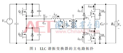
The LLC resonant converter is shown in Figure 1 [1]. Unlike conventional resonant converters, the two rectifier diodes on one rectifier bridge arm of the LLC converter are replaced by SR switches. The SR switch is frequency-modulated with the primary side switch to reduce the conduction loss of the secondary side switch.
Using the harmonic approximation method, the DC output voltage gain of the LLC resonant converter can be obtained as:
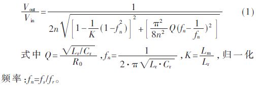
The corresponding gain curve of the resonant converter at different Q values ​​can be obtained from equation (1). As shown in Figure 2, when it works under different loads, the switching frequency varies within a small range, and there is no problem of light load regulation. If the inverter control is used, the operating frequency range will be wider, and the voltage may be out of balance. In this paper, the fixed frequency control is used to adjust the duty cycle or phase shift angle of the switching transistor drive signal to stabilize the output voltage according to the change of the load voltage.
1.2 Working mode analysis
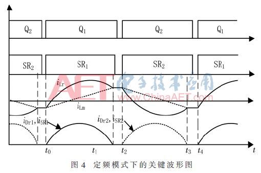
This paper uses the fixed frequency phase shift control mode, as shown in Figure 3.

That is, at the time of high voltage input, the SR switch is turned on in synchronization with the primary side switch because current flows through the secondary measured switching channel, has a small on-resistance, and the conduction loss of the secondary rectification is reduced. The rectifier current directly becomes zero before the SR switch needs to be turned off. Since the current flows through the series rectifier diode and the SR switch, the rectifier diode prevents the rectified current from being negative, allowing the SR switch to operate in the positive half cycle. When the switching frequency is less than and close to the resonant frequency, the LLC operates in the discontinuous mode. The LLC resonant converter operates in a similar manner to the conventional resonant converter, and will not be specifically described here. The key waveforms are shown in Figure 4.
When the input voltage of the converter is low, the phase shift control is adopted, that is, the secondary side SR switch controls the phase shift of the gate signal, so that the converter can obtain a high voltage gain without lowering the switching frequency. Due to the narrow operating frequency range of the converter, a small transformer can be selected to reduce the transformer core size and conduction loss to maximize efficiency throughout the load. The key waveforms in phase shift mode are shown in Figure 5.

Switch mode 1 (t0~t1): Q1 is turned on, the voltage on Lr is Vin-VCr, the resonant current flows from the drain through the source, and the cavity current iLr increases linearly. The energy difference between the resonant current and the exciting current is transferred to the load by secondary side rectification. Since SR2 is continuously turned on, the voltage applied across the magnetizing inductance is zero.
Switch Mode 2 (t1~t2): SR2 is turned off, and the energy stored by Cr to Lr is output to capacitor C0 through DR1 and SR2. The voltage across the transformer's magnetizing inductance is clamped, at which point VLm = nVout. The iLm increases linearly, and the cavity current iLr decreases with the slope of (Vin-VCr-nVout)/Lr, and finally equals the current on the magnetizing inductance, ie iLr=iLm.
Switch Mode 3 (t2~t3): Dr1 is turned off, because SR1 is continuously turned on, and the transformer secondary is not reflected to the primary side. The voltage on the resonant network composed of Lr and Lm is Vin-VCr, and Lr and Lm grow synchronously. The output filter capacitor C0 provides energy to the load.
Switch mode 4 (t3~t4): Q1 is off, Q2 is not open, and enters dead time. Since SR2 remains open, Cr continues to discharge Lr, and the cavity current increases linearly. At this point, the Q2 parasitic capacitance begins to discharge, preparing for the ZVS turn-on of Q2.
Switching mode 5 (t4~t5): Phase 5 is symmetric with Phase 1, and is not repeated here. The remaining switching time converter operating modes are symmetrical with the above.
2 LLC resonant converter design
2.1 Main circuit key parameter design
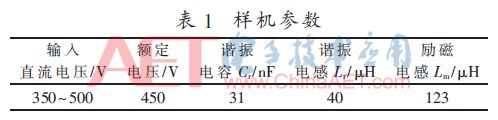
The optimal design of the resonant network parameters is an important part of determining whether the converter is reliable. The design parameters: the input voltage of the resonant converter is 350 V~500 V; the rated voltage Uin=450 V; the output voltage V0=200 V; fr=100 kHz. When the input is between 450 V and 500 V, the resonant converter operates near the resonant frequency. When the input is between 350 V and 450 V, the secondary SR is phase-shifted without reducing the switching frequency.
(1) Transformer ratio:

The gain range is from 0.91 to 1.30. When designing parameters, in addition to meeting the gain requirements, the original secondary side current RMS and frequency modulation range should be as small as possible. The prototype parameters are shown in Table 1.
2.2 Transformer design
Whether the transformer is designed to properly affect the efficiency and performance of the switching power supply. When the converter operates in fixed frequency mode, the LLC operates near the resonant frequency and the maximum flux density is:
It can be seen from equation (6) that D decreases as the input voltage increases. According to the previous analysis, during the phase shift, the voltage across the magnetizing inductance is zero, and the output voltage is increased by the fixed frequency shifting when the input voltage is lowered. The increase of D causes the amplitude of iLm to decrease. Since the LLC resonant converter has the maximum magnetic flux density at the minimum voltage input, the transformer can use a core as small as possible to reduce transformer core loss and increase power density.
In this design, the transformer adopts EI25 core with a core cross-sectional area Ae=0.41 cm2 and a magnetic flux density Bw=2 140 Gauss.
2.3 Software part design
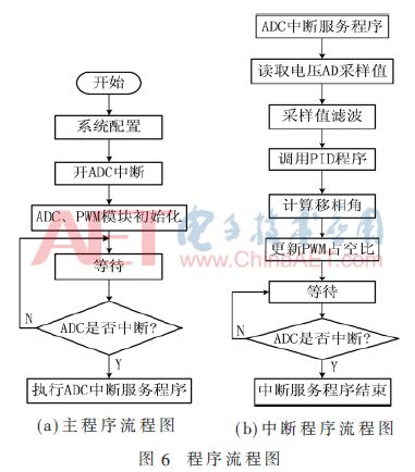
The main program flow chart and the ADC interrupt program flow chart correspond to (a) and (b) in Fig. 6, respectively, and the software performs the voltage closed loop adjustment while performing the secondary side phase shift to realize the high voltage output, so that the output voltage reaches a stable value. [4]. Since the DSP chip has an ADC module inside, the LEM sample feeds the output voltage back to the ADC module of the DSP, reads the sample in the AD interrupt program, reads the output signal and stores the sampled result, and then performs the PID control algorithm through digital filtering. The call is made to update the PWM drive signal according to the calculated error to the required control amount, and finally determine the phase angle [5, 6].
3 Simulation and experimental analysis
According to the above analysis and the parameter design of the prototype, the Saber simulation model is built, and the correctness and stability of the digital LLC resonant converter designed in this paper are preliminarily verified.
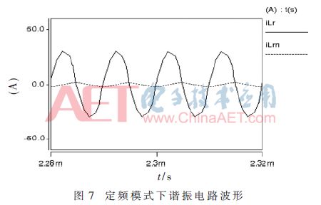
Figure 7 and Figure 8 are the resonant tank current waveforms of the LLC resonant converter in the fixed-frequency and phase-shift modes respectively. It can be seen that the magnetizing inductor has a small current flowing through it, so the conduction loss is higher on the premise that the primary side satisfies the ZVS turn-on. small. The difference between iLm and iLr in the load range can be maximized and output to the load through the secondary side rectification, which effectively improves the efficiency of the converter.

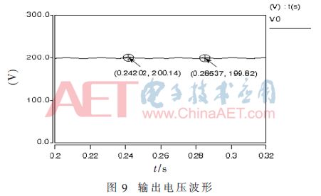
As can be seen from Figure 9, the load output voltage is about 200 V, the ripple amplitude is below 0.2 V, and the output voltage is relatively stable, meeting the accuracy requirements.
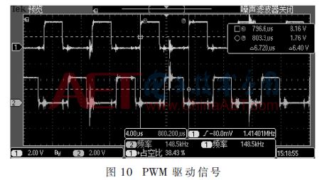
The key to the software part of the debugging process is to debug the PWM drive signal. Figure 10 shows the waveform of the PWM drive signal with the dead zone of the same bridge arm MOSFET. As can be seen from the figure, the PWM signal output of the driver circuit is 10 μs, that is, the switching frequency is 100 kHz, and the dead time is about 300 ns. Consistent with the parameters of the design prototype, it can effectively avoid simultaneous conduction of the same bridge arm. phenomenon.
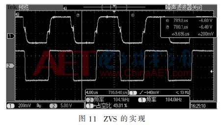
After theoretical analysis and debugging results, as long as the lagging bridge arm can achieve ZVS, all the switching tubes of the charging module will realize ZVS. As shown in Figure 11, when the MOS transistor of the lag bridge arm is turned off, the Vds rises compared to the current zero voltage turn-off. Due to the Miller effect and the leakage inductance, Vds will have an acceleration phase before it rises to the maximum value. When the Vds of the MOSFET of the lag bridge arm drops to zero, the PWM drive signal is turned on, achieving zero voltage turn-on.
The hardware and software parts are tested separately, and then the system can be adjusted. After the system is successfully adjusted, the efficiency of different input loads is tested. The efficiency curve is shown in Figure 12. The experiment proves that the LLC resonant converter can achieve high efficiency operation in the full load range, which verifies the reliability of the scheme.

4 Conclusion
This paper introduces a digital charging scheme based on LLC resonant converter. By performing fixed frequency and phase shift control on different input voltages, the conduction loss of the primary side is effectively reduced, and a high voltage gain is obtained. The designed circuit is verified by Saber simulation software, and finally the experiment is carried out and its performance index is tested, and the relevant waveform is analyzed in detail. The results show that all the switching tubes of the charging prototype can realize ZVS under a wide range of voltage input, which reduces the switching loss and the efficiency of the prototype reaches over 92%. It verifies the correctness of the theoretical analysis and meets the charging requirements of the charger.
72V20Ah Lithium Ion Battery,Electric Scooter Lifepo4 Battery Pack,Lithium Battery For Electric Motorcycle,Lithium Battery For Electric Bike
Jiangsu Zhitai New Energy Technology Co.,Ltd , https://www.jszhitaienergy.com