The growth of handheld multimedia devices has greatly changed the positioning needs of terminal multimedia chip suppliers for their products. The IC design goals of these chip providers are no longer just for one or two multimedia codecs. Consumers hope that their mobile devices can use different devices to play media, can use different standards for encoding, and can download or receive media data from different devices. Video decoders and encoder engines must meet a variety of needs and have advantages in area and power consumption.
1. Traditional RTL method of designing video acceleration engine The design of the previous generation video ASIC mainly encodes and decodes MPEG-2, because this is the DVD standard. Some video ASICs also support MPEG-1 for VCD (Video CD) playback. In most cases, MPEG-2 encoders and decoders use RTL design methods. A typical MPEG-2 video ASIC architecture is shown in Figure 1, which includes the video subsystem, main controller, and on-chip memory composed of various RTL modules.
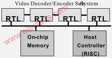
Figure 1 The MPEG-2 video ASIC architecture uses a hard-wired RTL architecture to support multiple video standards. However, this also means that each video standard requires a dedicated RTL module to implement. Using hardwired RTL modules to implement a multi-standard video acceleration engine has certain limitations. Whether it is to implement a new video standard, update an existing standard, or eliminate failures, chip processing is required.
2. Advantages of using a processor as a video acceleration engine. A programmable processor can meet the flexibility requirements of multiple video standards. Compared with the RTL module design method, the programmable processor has the following advantages: First, it is easy to interface the codec with the processor; Second, it meets the requirements of the new video standard, updates the existing codec, or uses software methods The fault can also be modified after the chip is cast; the third is that the performance of the video codec can be easily improved by software update.
However, traditional 32-bit processors have performance bottlenecks because they are designed for general-purpose code, not for video acceleration engines. Embedded DSP is not specifically tailored for video, but includes hardware features, instructions and interfaces, specifically used in the field of general-purpose DSP. Therefore, in order to implement video codecs on traditional RISC and DSP processors, these processors must be run at very high speeds (Mhz), requiring a large amount of memory space, and therefore requiring large power consumption, which is not suitable Portable applications.
By studying the amount of calculation required for a video kernel program, it can be seen at a glance. For example, an absolute difference accumulation operation SAD, which is a commonly used method of motion estimation in most video encoding algorithms. The SAD algorithm will find the motion of the macroblock in two consecutive video frames. For this, the cumulative sum of the absolute differences between the corresponding pixel values ​​in each group of the two macroblocks needs to be calculated.
The following C code gives a simple implementation of the SAD core algorithm:
for (row = 0; row <numrows; row ++) {
for (col = 0; col <numcols; col ++) {
accum + = abs (macroblk1 [row] [col]-macroblk2 [row] [col]);
} / * column loop * /
} / * row loop * /
The basic calculation method of the SAD core algorithm is shown in Figure 2. As shown in the figure, the SAD core algorithm first performs the subtraction operation, then takes the absolute value, and finally accumulates the previous results.
Figure 2 The main calculation method of difference absolute value accumulation (SAD) Calculating a SAD operation consisting of two 16x16 macro blocks on a RISC processor requires 256 subtraction operations, 256 absolute value operations, and 256 accumulation operations. 768 arithmetic operations, which does not include the fetch and store operations required for data transfer. Since this requires operations on all macroblocks of each frame, as the resolution increases, the video frames increase, making the calculation cost extremely expensive.
In fact, for a general general-purpose RISC processor (including some DSP instructions, such as multiply instructions and multiply-accumulate instructions), the execution of an H.264 benchmark decoding algorithm requires 250 MHz of performance (CIF resolution) while executing An H.264 benchmark encoding algorithm requires performance (CIF resolution) of more than 1 GHz. To complete the above calculations, the processor core alone requires 500mW of power consumption, not to mention the power consumption used by other components of the memory access and video SOC.
3. Configurable processor method A more effective way to implement the SAD core algorithm on a processor is to establish a special instruction for "subtraction-absolute value-addition". This will greatly reduce the cost of arithmetic operations. For a 16x16 macroblock, the number of operations will be reduced from 768 to 256. Moreover, because a single functional component can be used to achieve the fusion operation of multiple simple arithmetic operations, the above operation can be completed in one instruction cycle, which is equivalent to the original 256 cycles. Users cannot add instructions to a standard 32-bit RISC processor, but they can add special instructions to a configurable processor. Configurable processors allow designers to select relevant configuration commands from the Configurable Options menu to expand processor functions, including adding special instructions, register files, and interfaces.
The following are configuration and expansion options provided by modern configurable processors (such as Tensilica's Xtensa processors), which is not possible with traditional fixed-mode processors.
(i) Configuration options: The options menu includes the following items:
a. Instructions that the designer needs or does not need. For example, 16x16 multiplication or multiply-accumulate, shift, floating point instructions, etc.
b. Zero-overhead loop, five-level or seven-level pipeline, local data loading or the number of storage components, etc.
c. Whether memory protection, memory address translation or memory management unit (MMU) is required
d. With or without system bus interface e. System bus width and local memory interface width f. Local (tightly coupled) memory size and number.
g. Number of interrupts, type of interrupt and priority of interrupt.
(ii) Expansion options: add the functional parts defined by the designer himself, including:
a. Registers and register files.
b. Multi-cycle, arbitrated complex instruction function part.
c. Single instruction flow and multiple data flow SIMD functional components.
d. Change the single-launch processor to a multi-launch processor.
e. User-defined interface, which can directly read and write data path, for example, the processor core port or pin like GPIO (General Purpose Input / Output) pin, used to extend the queue interface of the first-in first-out FIFO queue (can Interface with other logic or processor cores).
The benefit of configuration options is to allow designers to build a processor of a moderate size by selecting only the options relevant to their application and be able to meet their specific applications. The advantage of the extended option is to allow designers to customize the processor according to the application, including the establishment of special instructions, register files, functional components and related interfaces, used to accelerate the execution of system application algorithms.
4. The key to supporting the configurable and extensible automation software development tool kit is not only the ability to automatically generate pre-verified RTL code for designers to customize the processor (including all system expansion functions), but also to automatically generate complete software Tools include a development tool suite optimized for the processor, an instruction set simulator based on clock cycles, and system models.
This automation means that the compiler is aware of new instructions, related registers, and register files added by the designer. Therefore, the compiler can schedule user-defined instructions and perform register allocation operations. Similarly, in addition to the basic registers of the processor itself, software developers can understand the registers and register files defined by the designer during debugging. At the same time, software developers can use the instruction set simulator to simulate new instructions defined by the designer. The RTOS port and system model of the real-time operating system related to the processor can also be automatically generated. Tensilica's software tools can automatically generate the above software tools within an hour, which is a core commitment to users who use configurable processors to be able to perform operations such as SAD operations without using RTL.
5. Use a configurable processor to build a video acceleration engine and build a multi-operation functional unit. It is a hassle to add a fusion operation like SAD to a configurable processor. A new instruction called "sub.abs.ac" can complete the "subtraction-absolute value-accumulation" operation. This new instruction can turn the operation in Figure 2 into the complex operation in Figure 3.
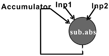
Figure 3 Using the new instruction to calculate the "subtraction-absolute value-accumulation" operation After adding this instruction to the processor, the C compiler can recognize this new "sub.abs.ac" instruction and schedule related instructions; the scheduler The internal signals used by the "sub.abs.ac" feature will be displayed; the assembler can process this new instruction; the instruction set simulator ISS can simulate in clock cycle mode.
The schematic diagram of the data path after the new dedicated video function component is inserted into the processor is shown in Figure 4. Note that in addition to generating functional component logic, hardware generation tools can also automatically insert feed-forward paths, control logic, and bypass logic to interconnect new functional components with other logic in the data path.
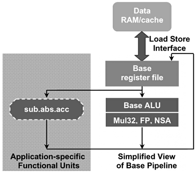
Figure 4 The simplified data path diagram after inserting sub.abs.ac video-specific functional components. The SAD algorithm described by the C code with new instructions is as follows:
for (row = 0; row <numrows; row ++) {for (col = 0; col <numcols; col ++) {
sub.abs.ac (accum, macroblk1 [row] [col], macroblk2 [row] [col]);
} / * column loop * /
} / * row loop * /
As mentioned earlier, for a 16x16 macroblock, the number of operands in the main loop of the program is reduced to 256 after adding new instructions (ie numrows = numcols = 16).
6. The SAD program in front of the SIMD function unit that establishes a single instruction stream and multiple data streams can be further optimized. The inner loop in the program does the same calculation for 16 columns in the macro block. This is ideal for SIMD (Single Instruction Multiple Data) functional components. The corresponding instruction "sub.abs.ac16" performs sub.abs.ac operations for 16 pixels at the same time, as shown in Figure 5.
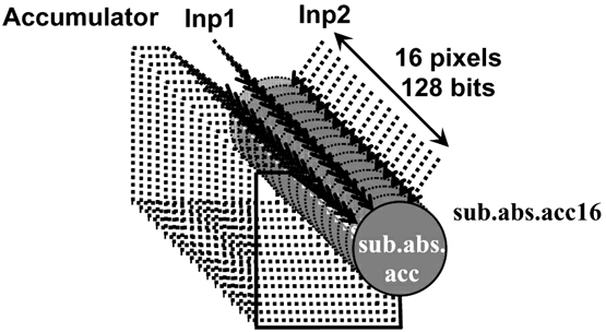
Figure 5 The single-instruction stream multi-data stream calculation operation of sub.abs.ac instructions for 16 pixels simultaneously. The corresponding C language process is called sub.abs.ac16. The SAD kernel C program code rewritten using this process name is as follows:
for (row = 0; row <numrows; row ++) {
sub.abs.ac16 (accum, macroblk1 [row], macroblk2 [row]);
} / * row loop * /
The rewritten SAD kernel program was reduced from 768 arithmetic operations to only 16 arithmetic operations.
However, only the above C program code is not enough. Because the instruction sub.abs.ac16 needs to read 128-bit data from two macro blocks, this requires two aspects of support: a 128-bit register file and a wide data bit fetch / store interface, configurable The processors all support these functions.
7. Create a custom register file. In the Xtensa configurable processor, indicating that a custom register file of any width is as simple as writing a line of program. For example, a procedural statement called "myRegFile128" creates a register file with a width of 128 bits, a length of 4, and a corresponding new C data type. "MyRegFile128" can be used to describe variables in C / C ++ program code. The software tool also establishes a "MOVE" operation, which is used to convert various C data types into new custom data types. Therefore, the SAD kernel C program code after using the sub.abs.ac16 process and the new register file is as follows:
for (row = 0; row <numrows; row ++) {
myRegFile128 mblk1, mblk2;
mblk1 = macroblk1 [row];
mblk2 = macroblk2 [row];
sub.abs.ac16 (accum, mblk1, mblk2);
} / * row loop * /
Now the C / C ++ compiler will generate a MOVE instruction to move the data from the general C data type to the custom C data type "myRegFile128" and allocate registers for the new register file.
8. Establish a high-data-bandwidth load / store interface In order to perform data access to high-bandwidth custom register files (and corresponding single instruction stream multiple data stream SIMD functional components), the processor should have high-bandwidth data load / store operation capabilities. For configurable processors, designers can specify custom load and store operation instructions and directly complete high-bandwidth load / store data operations on custom register files. Then, the compiler automatically generates a load / store instruction corresponding to the high-bandwidth load / store interface.
The updated processor data path is shown in Figure 6. The hardware generation tool generates high-bandwidth custom register files, load / store interfaces related to data storage, and corresponding feedforward logic, control logic, and bypass logic. The hardware tool also generates corresponding hardware logic for moving data from the reference register file to the user-defined register file.
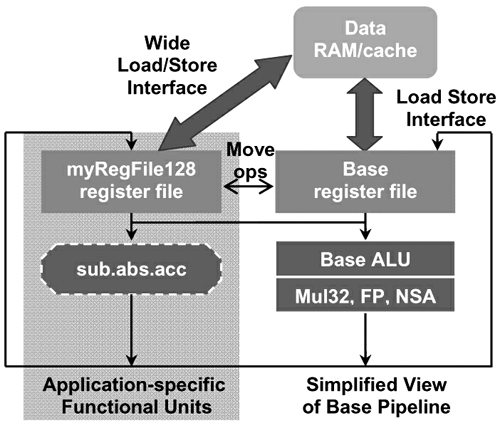
Figure 6: Data path inserted into register file and high-bandwidth load / store interface 9. Simultaneous load or store operation while updating address Xtensa configurable processor allows the user to create another very useful functional extension, that is, to create an instruction that can be completed at the same time Address update operation and data load / store operation. The new load / store operation instruction created can complete the following functions concurrently: Load A1 ↠Memory (Addr1); Addr1 = Addr1 + IndexUpdate
This instruction can complete "back-to-back" load / store operations without requiring special instructions to update the address.
10. Establish a first-in first-out (FIFO) interface and general-purpose input / output ports. Both video and audio are streaming media and require fast data access to the processor. Traditional processors are limited by the system bus interface, and the loading and storage access to all data before data operations are performed.
To support streaming data / output operations, Xtensa configurable processors allow designers to define first-in first-out (FIFO) interfaces and general-purpose input / output (GPIO) ports for direct read and write access to data paths. FIFO and GPIO ports can be any data width (up to 1024 bits), the number is unlimited (each can contain 1024 FIFO and GPIO ports). These high-bandwidth interfaces can be directly connected to the data path to provide very high data throughput. Data is read, processed, and written through the processor core, which is very important for multimedia and network applications.
The data path with FIFO interface and GPIO port is shown in Figure 7. The processor can perform the following operations: first fetch the data from the two FIFOs (in case both FIFO queues are not empty), then calculate a complex operation (such as a multiply-accumulate round operation), and finally The result is pushed into the output FIFO (while ensuring that the FIFO queue is not full). Then, the hardware generation tool generates corresponding interface signals, control logic, bypass logic, etc .; generates complete RTL code for the configured processor. The software generation tool generates a complete set of compiler tools, and an instruction set simulator ISS with a precise clock cycle for simulating new instructions. Note that this ability for designers to define FIFO interfaces and GPIO ports is unique to Xtensa's configurable processors.
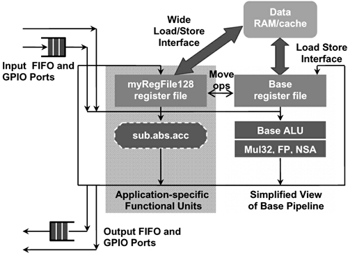
Figure 7 High-speed communication using custom first-in first-out (FIFO) interface and general-purpose input-output (IO) port 11. Accelerate the execution of complex control-intensive code The number and complexity of control codes in multimedia applications have increased significantly, making the data in the program Intensive operations are approximately equivalent to computing time. For example, the key part of the H.264 main program decoder is the CABAC (Context-Related Binary Arithmetic Coding) algorithm. The algorithm is almost entirely a control flow decision tree with data calculation and data comparison.
Due to the very high computational complexity, most traditional processors use a dedicated RTL accelerator to complete the CABAC algorithm. However, the CABAC algorithm can be implemented more efficiently by adding a set of dedicated instructions on the configurable processor. The advantage of this implementation method is to avoid the non-stop exchange of data between the processor and the RTL accelerator. Another advantage of using a configurable processor is the use of instruction extension technology. Since the dedicated hardware is inside the processor, the hardware and software interfaces can be better divided.
12. Summary Modern configurable and scalable processors are ideal for building custom video and audio engines. Tensilica provides related video and audio IP as SOC modules, including HiFi 2 audio engine, diamond series standard 38xVDO (video) multi-standard and multi-resolution video methods. The matching software codec is very important. HiFi 2 audio engine and related software can complete most popular audio codecs, such as MP3, AAC, WMA, etc. Similarly, Diamond 38xVDO video acceleration engine and corresponding encoder and decoder software can implement H.264 (including Baseline, Main and profiles), MPEG-4 (SP and ASP), MPEG-2, VC-1 / WM9 And other standards. These video technologies cover various resolutions from QCIF to CIF and SD, with low power consumption and small area.
1. Traditional RTL method of designing video acceleration engine The design of the previous generation video ASIC mainly encodes and decodes MPEG-2, because this is the DVD standard. Some video ASICs also support MPEG-1 for VCD (Video CD) playback. In most cases, MPEG-2 encoders and decoders use RTL design methods. A typical MPEG-2 video ASIC architecture is shown in Figure 1, which includes the video subsystem, main controller, and on-chip memory composed of various RTL modules.
Figure 1 The MPEG-2 video ASIC architecture uses a hard-wired RTL architecture to support multiple video standards. However, this also means that each video standard requires a dedicated RTL module to implement. Using hardwired RTL modules to implement a multi-standard video acceleration engine has certain limitations. Whether it is to implement a new video standard, update an existing standard, or eliminate failures, chip processing is required.
2. Advantages of using a processor as a video acceleration engine. A programmable processor can meet the flexibility requirements of multiple video standards. Compared with the RTL module design method, the programmable processor has the following advantages: First, it is easy to interface the codec with the processor; Second, it meets the requirements of the new video standard, updates the existing codec, or uses software methods The fault can also be modified after the chip is cast; the third is that the performance of the video codec can be easily improved by software update.
However, traditional 32-bit processors have performance bottlenecks because they are designed for general-purpose code, not for video acceleration engines. Embedded DSP is not specifically tailored for video, but includes hardware features, instructions and interfaces, specifically used in the field of general-purpose DSP. Therefore, in order to implement video codecs on traditional RISC and DSP processors, these processors must be run at very high speeds (Mhz), requiring a large amount of memory space, and therefore requiring large power consumption, which is not suitable Portable applications.
By studying the amount of calculation required for a video kernel program, it can be seen at a glance. For example, an absolute difference accumulation operation SAD, which is a commonly used method of motion estimation in most video encoding algorithms. The SAD algorithm will find the motion of the macroblock in two consecutive video frames. For this, the cumulative sum of the absolute differences between the corresponding pixel values ​​in each group of the two macroblocks needs to be calculated.
The following C code gives a simple implementation of the SAD core algorithm:
for (row = 0; row <numrows; row ++) {
for (col = 0; col <numcols; col ++) {
accum + = abs (macroblk1 [row] [col]-macroblk2 [row] [col]);
} / * column loop * /
} / * row loop * /
The basic calculation method of the SAD core algorithm is shown in Figure 2. As shown in the figure, the SAD core algorithm first performs the subtraction operation, then takes the absolute value, and finally accumulates the previous results.
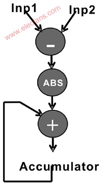
Figure 2 The main calculation method of difference absolute value accumulation (SAD) Calculating a SAD operation consisting of two 16x16 macro blocks on a RISC processor requires 256 subtraction operations, 256 absolute value operations, and 256 accumulation operations. 768 arithmetic operations, which does not include the fetch and store operations required for data transfer. Since this requires operations on all macroblocks of each frame, as the resolution increases, the video frames increase, making the calculation cost extremely expensive.
In fact, for a general general-purpose RISC processor (including some DSP instructions, such as multiply instructions and multiply-accumulate instructions), the execution of an H.264 benchmark decoding algorithm requires 250 MHz of performance (CIF resolution) while executing An H.264 benchmark encoding algorithm requires performance (CIF resolution) of more than 1 GHz. To complete the above calculations, the processor core alone requires 500mW of power consumption, not to mention the power consumption used by other components of the memory access and video SOC.
3. Configurable processor method A more effective way to implement the SAD core algorithm on a processor is to establish a special instruction for "subtraction-absolute value-addition". This will greatly reduce the cost of arithmetic operations. For a 16x16 macroblock, the number of operations will be reduced from 768 to 256. Moreover, because a single functional component can be used to achieve the fusion operation of multiple simple arithmetic operations, the above operation can be completed in one instruction cycle, which is equivalent to the original 256 cycles. Users cannot add instructions to a standard 32-bit RISC processor, but they can add special instructions to a configurable processor. Configurable processors allow designers to select relevant configuration commands from the Configurable Options menu to expand processor functions, including adding special instructions, register files, and interfaces.
The following are configuration and expansion options provided by modern configurable processors (such as Tensilica's Xtensa processors), which is not possible with traditional fixed-mode processors.
(i) Configuration options: The options menu includes the following items:
a. Instructions that the designer needs or does not need. For example, 16x16 multiplication or multiply-accumulate, shift, floating point instructions, etc.
b. Zero-overhead loop, five-level or seven-level pipeline, local data loading or the number of storage components, etc.
c. Whether memory protection, memory address translation or memory management unit (MMU) is required
d. With or without system bus interface e. System bus width and local memory interface width f. Local (tightly coupled) memory size and number.
g. Number of interrupts, type of interrupt and priority of interrupt.
(ii) Expansion options: add the functional parts defined by the designer himself, including:
a. Registers and register files.
b. Multi-cycle, arbitrated complex instruction function part.
c. Single instruction flow and multiple data flow SIMD functional components.
d. Change the single-launch processor to a multi-launch processor.
e. User-defined interface, which can directly read and write data path, for example, the processor core port or pin like GPIO (General Purpose Input / Output) pin, used to extend the queue interface of the first-in first-out FIFO queue (can Interface with other logic or processor cores).
The benefit of configuration options is to allow designers to build a processor of a moderate size by selecting only the options relevant to their application and be able to meet their specific applications. The advantage of the extended option is to allow designers to customize the processor according to the application, including the establishment of special instructions, register files, functional components and related interfaces, used to accelerate the execution of system application algorithms.
4. The key to supporting the configurable and extensible automation software development tool kit is not only the ability to automatically generate pre-verified RTL code for designers to customize the processor (including all system expansion functions), but also to automatically generate complete software Tools include a development tool suite optimized for the processor, an instruction set simulator based on clock cycles, and system models.
This automation means that the compiler is aware of new instructions, related registers, and register files added by the designer. Therefore, the compiler can schedule user-defined instructions and perform register allocation operations. Similarly, in addition to the basic registers of the processor itself, software developers can understand the registers and register files defined by the designer during debugging. At the same time, software developers can use the instruction set simulator to simulate new instructions defined by the designer. The RTOS port and system model of the real-time operating system related to the processor can also be automatically generated. Tensilica's software tools can automatically generate the above software tools within an hour, which is a core commitment to users who use configurable processors to be able to perform operations such as SAD operations without using RTL.
5. Use a configurable processor to build a video acceleration engine and build a multi-operation functional unit. It is a hassle to add a fusion operation like SAD to a configurable processor. A new instruction called "sub.abs.ac" can complete the "subtraction-absolute value-accumulation" operation. This new instruction can turn the operation in Figure 2 into the complex operation in Figure 3.
Figure 3 Using the new instruction to calculate the "subtraction-absolute value-accumulation" operation After adding this instruction to the processor, the C compiler can recognize this new "sub.abs.ac" instruction and schedule related instructions; the scheduler The internal signals used by the "sub.abs.ac" feature will be displayed; the assembler can process this new instruction; the instruction set simulator ISS can simulate in clock cycle mode.
The schematic diagram of the data path after the new dedicated video function component is inserted into the processor is shown in Figure 4. Note that in addition to generating functional component logic, hardware generation tools can also automatically insert feed-forward paths, control logic, and bypass logic to interconnect new functional components with other logic in the data path.
Figure 4 The simplified data path diagram after inserting sub.abs.ac video-specific functional components. The SAD algorithm described by the C code with new instructions is as follows:
for (row = 0; row <numrows; row ++) {for (col = 0; col <numcols; col ++) {
sub.abs.ac (accum, macroblk1 [row] [col], macroblk2 [row] [col]);
} / * column loop * /
} / * row loop * /
As mentioned earlier, for a 16x16 macroblock, the number of operands in the main loop of the program is reduced to 256 after adding new instructions (ie numrows = numcols = 16).
6. The SAD program in front of the SIMD function unit that establishes a single instruction stream and multiple data streams can be further optimized. The inner loop in the program does the same calculation for 16 columns in the macro block. This is ideal for SIMD (Single Instruction Multiple Data) functional components. The corresponding instruction "sub.abs.ac16" performs sub.abs.ac operations for 16 pixels at the same time, as shown in Figure 5.
Figure 5 The single-instruction stream multi-data stream calculation operation of sub.abs.ac instructions for 16 pixels simultaneously. The corresponding C language process is called sub.abs.ac16. The SAD kernel C program code rewritten using this process name is as follows:
for (row = 0; row <numrows; row ++) {
sub.abs.ac16 (accum, macroblk1 [row], macroblk2 [row]);
} / * row loop * /
The rewritten SAD kernel program was reduced from 768 arithmetic operations to only 16 arithmetic operations.
However, only the above C program code is not enough. Because the instruction sub.abs.ac16 needs to read 128-bit data from two macro blocks, this requires two aspects of support: a 128-bit register file and a wide data bit fetch / store interface, configurable The processors all support these functions.
7. Create a custom register file. In the Xtensa configurable processor, indicating that a custom register file of any width is as simple as writing a line of program. For example, a procedural statement called "myRegFile128" creates a register file with a width of 128 bits, a length of 4, and a corresponding new C data type. "MyRegFile128" can be used to describe variables in C / C ++ program code. The software tool also establishes a "MOVE" operation, which is used to convert various C data types into new custom data types. Therefore, the SAD kernel C program code after using the sub.abs.ac16 process and the new register file is as follows:
for (row = 0; row <numrows; row ++) {
myRegFile128 mblk1, mblk2;
mblk1 = macroblk1 [row];
mblk2 = macroblk2 [row];
sub.abs.ac16 (accum, mblk1, mblk2);
} / * row loop * /
Now the C / C ++ compiler will generate a MOVE instruction to move the data from the general C data type to the custom C data type "myRegFile128" and allocate registers for the new register file.
8. Establish a high-data-bandwidth load / store interface In order to perform data access to high-bandwidth custom register files (and corresponding single instruction stream multiple data stream SIMD functional components), the processor should have high-bandwidth data load / store operation capabilities. For configurable processors, designers can specify custom load and store operation instructions and directly complete high-bandwidth load / store data operations on custom register files. Then, the compiler automatically generates a load / store instruction corresponding to the high-bandwidth load / store interface.
The updated processor data path is shown in Figure 6. The hardware generation tool generates high-bandwidth custom register files, load / store interfaces related to data storage, and corresponding feedforward logic, control logic, and bypass logic. The hardware tool also generates corresponding hardware logic for moving data from the reference register file to the user-defined register file.
Figure 6: Data path inserted into register file and high-bandwidth load / store interface 9. Simultaneous load or store operation while updating address Xtensa configurable processor allows the user to create another very useful functional extension, that is, to create an instruction that can be completed at the same time Address update operation and data load / store operation. The new load / store operation instruction created can complete the following functions concurrently: Load A1 ↠Memory (Addr1); Addr1 = Addr1 + IndexUpdate
This instruction can complete "back-to-back" load / store operations without requiring special instructions to update the address.
10. Establish a first-in first-out (FIFO) interface and general-purpose input / output ports. Both video and audio are streaming media and require fast data access to the processor. Traditional processors are limited by the system bus interface, and the loading and storage access to all data before data operations are performed.
To support streaming data / output operations, Xtensa configurable processors allow designers to define first-in first-out (FIFO) interfaces and general-purpose input / output (GPIO) ports for direct read and write access to data paths. FIFO and GPIO ports can be any data width (up to 1024 bits), the number is unlimited (each can contain 1024 FIFO and GPIO ports). These high-bandwidth interfaces can be directly connected to the data path to provide very high data throughput. Data is read, processed, and written through the processor core, which is very important for multimedia and network applications.
The data path with FIFO interface and GPIO port is shown in Figure 7. The processor can perform the following operations: first fetch the data from the two FIFOs (in case both FIFO queues are not empty), then calculate a complex operation (such as a multiply-accumulate round operation), and finally The result is pushed into the output FIFO (while ensuring that the FIFO queue is not full). Then, the hardware generation tool generates corresponding interface signals, control logic, bypass logic, etc .; generates complete RTL code for the configured processor. The software generation tool generates a complete set of compiler tools, and an instruction set simulator ISS with a precise clock cycle for simulating new instructions. Note that this ability for designers to define FIFO interfaces and GPIO ports is unique to Xtensa's configurable processors.
Figure 7 High-speed communication using custom first-in first-out (FIFO) interface and general-purpose input-output (IO) port 11. Accelerate the execution of complex control-intensive code The number and complexity of control codes in multimedia applications have increased significantly, making the data in the program Intensive operations are approximately equivalent to computing time. For example, the key part of the H.264 main program decoder is the CABAC (Context-Related Binary Arithmetic Coding) algorithm. The algorithm is almost entirely a control flow decision tree with data calculation and data comparison.
Due to the very high computational complexity, most traditional processors use a dedicated RTL accelerator to complete the CABAC algorithm. However, the CABAC algorithm can be implemented more efficiently by adding a set of dedicated instructions on the configurable processor. The advantage of this implementation method is to avoid the non-stop exchange of data between the processor and the RTL accelerator. Another advantage of using a configurable processor is the use of instruction extension technology. Since the dedicated hardware is inside the processor, the hardware and software interfaces can be better divided.
12. Summary Modern configurable and scalable processors are ideal for building custom video and audio engines. Tensilica provides related video and audio IP as SOC modules, including HiFi 2 audio engine, diamond series standard 38xVDO (video) multi-standard and multi-resolution video methods. The matching software codec is very important. HiFi 2 audio engine and related software can complete most popular audio codecs, such as MP3, AAC, WMA, etc. Similarly, Diamond 38xVDO video acceleration engine and corresponding encoder and decoder software can implement H.264 (including Baseline, Main and profiles), MPEG-4 (SP and ASP), MPEG-2, VC-1 / WM9 And other standards. These video technologies cover various resolutions from QCIF to CIF and SD, with low power consumption and small area.
Basketball Air Pump,Basketball Pump Near Me ,Best Basketball Pump,Electric Basketball Pump
SHENZHEN SMARTNEWO TECHNOLOGY CO,. LTD , https://www.newopump.com