0 Preface
Due to the increasing application of FPGAs in embedded system development, some embedded CPUs, such as STM32, have reduced the cost and reduced the package size. There is no external CPU read/write bus, but only some such as SPI and I2C. Interface. Moreover, in the application, there is often data to be configured into the FPGA, such as application configuration registers in the FPGA, and configuration entries, etc., all require CPU configuration. The amount of data in this data is small and the speed is not very high, so it is suitable for configuration with the I2C bus.
The I2C bus is a serial bus designed and controlled by Philips to control the internal IC bidirectional two-wire. The main feature is that the interface signal line is less, but the data transfer rate is not very high, and its high-speed mode is 3.4Mb/s. It is suitable for configuring the FPGA. In normal applications, the embedded CPU acts as the master of the MASTER mode and the FPGA acts as the slave to the SLAVE mode. By using the I2C bus, the connection between the CPU and the FPGA is reduced, and the embedded CPU generally has an I2C bus controller, which simplifies the communication hardware circuit between the CPU and the FPGA.
1 Analysis and design of the overall structure of the I2C SLAVE mode
The I2C bus requires two signal lines, one serial data line SDA, and one serial clock line SCL. The data is transmitted serially. It is a multi-master bus that can detect and arbitrate if two or more masters transmit data simultaneously. To simplify design and meet application requirements, the design implements a subset of a standard I2C bus. Complete 1 byte single read and write and continuous read and write functions. So this requires only one master on the I2C bus in the application, and the FPGA logic can only be used as a slave. The two signal lines of the I2C bus are open-drain and must be connected with an external pull-up resistor to ensure that the bus is high when the bus is idle. I2C read and write timing diagram is shown in Figure 1.
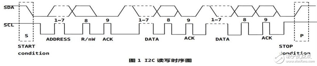
As can be seen from Figure 1, the starting condition of the bus is that SDA is pulled low to produce a falling edge when SCL is high. The bus is stopped when SCL is high and a rising edge is generated by the pull-up resistor. In fast mode, the SCL clock frequency is 400KHz maximum, the SCL clock has a minimum period of 1.3μs, and the SCL clock has a minimum period of 0.6μs. At the input, the input filter must suppress the glitch width. The maximum value is 50ns. Since SCL is generated by the built-in I2C module of the master CPU, the timing of the SCL is definitely satisfactory. For FPGAs to sample SCL and SDA signals, the FPGA should have a sampling clock frequency of at least 2 times the SCL frequency. In addition, the maximum value of the suppressed glitch width is 50 ns. When the system clock of the FPGA is 100 MHz, the port samples the signal at a frequency of 100 MHz, which is much larger than the 400 kHz of the SCl in the fast mode, and the suppressed glitch will also be 5 clock cycles. Internal processing. Moreover, the internal logic of the FPGA generally works above 100MHz, so the system clock of the I2C module can directly use the system clock of the FPGA, which can save the clock conversion module and simplify processing. When the I2C bus reads the FPGA, after the bus master sends the first byte, the FPGA responds with an ACK, and then the FPGA outputs the corresponding data. Therefore, the FPGA logic starts to issue an ACK, and the FPGA internally searches. Address and read the corresponding data, when the SCL clock frequency is 400KHz maximum, the FPGA system clock is 100MHz, then the FPGA internal logic has about 250 clock cycles of addressing time, this time is completely sufficient. The overall structure of I2C SLAVEmode is shown in Figure 2.
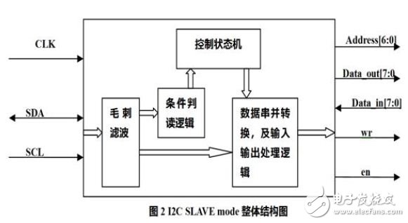
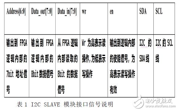
The interface signal is described in Table 1.
Super Bright & Power Saving: 30W handheld Led Work Light, 1500 Lumen, replace 200W traditional halogen bulb by 30W COB LED and save 80% on electricity bill of lighting
LED Work Lights Portable & Flexibility: Because the rechargeable flood light is cordless. with a 180 degree adjustable lamp stand. So you can put it in anywhere just you like. led portable Work Light hanging on truck or hand held. Even on the ground, in the basement, garage or garden at night
3 Modes & Waterproof: Press the switch on button turn on the work light rechargeable: High, Low, Strobe Brightness Mode. IP65 Waterproof rating, ensure the Rechargeable Led Work Light works fine in rainy days
LED Work Light Rechargeable & Battery Powered: Powered by 2 18650 lithium-ion rechargeable batteries(included) or 4 AA batteries(not included), equipped a USB cable allows for quick and convenient charging. Also Serve as a convenient power bank for charging your phone and other devices in emergency
Portable Flood Light Widely Used: Camping, Hiking, Fishing, Barbecue, Car Repairing, Truck, Workshop, Construction Site, Job Site Lighting, Exploring and more Outdoor Activities
Work Light
Led Work Light,Rechargeable Work Light ,Work Lamp,Rechargeable Led Work Light
Ningbo Wason Lighting Technology Co.,Ltd , https://www.wasonlight.com