Transmission line theory explains that the signal source output is not affected by impedance changes that occur along the path between the component's input and output. When an AC signal travels through a transmission line, any change in impedance causes part of the signal to reflect back toward the source, while the remaining portion continues to the receiver. The larger the impedance mismatch, the more significant the reflection, which can lead to signal distortion and reduced signal integrity.
Impedance variations are influenced by several factors, such as wire width, spacing between adjacent wires or components, and the distance from the reference plane. On a printed circuit board (PCB), these changes may not always be immediately visible. A practical approach is to review the PCB layout or system diagram to identify potential problem areas that might require further analysis using simulation tools. While examining the design, it’s important to trace the signal path from the source to the receiver, check for compliance with the guidelines listed in Table 1, and pay attention to the critical points discussed below.
**Table 1: Inspection Guidelines for Minimizing Reflections**
| Single-Ended | Differential Type |
|--------------|-------------------|
| Wire width must remain constant | Differential wire spacing (coupling) and wire width must remain constant |
| Spacing between wires and other devices should be at least three times the wire width | Same as above |
| A consistent reference plane must be maintained throughout the conductor's length | Same as above |
These guidelines are not always strictly required, but they are commonly violated in specific areas, such as:
- **BGA traces**, especially when dealing with multiple I/O devices that connect to internal rows or columns.
- **Vias** need special attention to ensure a continuous reference plane as signals pass through different PCB layers.
- **Online devices and connectors** often introduce impedance mismatches due to differences in package size compared to the transmission line.
To maintain consistent impedance, carefully manage trace width and spacing when routing to and from BGA devices. Figure 1 illustrates some common considerations from the DS125DF1610 16-channel 12.5Gbps retimer data sheet (a 196-pin BGA device).
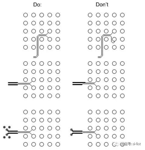
Starting from the top, the first rule combination in Figure 1 shows how to properly route differential traces within BGA rows and columns. The second set of rules highlights a technique called "necking," where a narrower trace may be used under the BGA. This is done symmetrically, ensuring the neck length matches the differential pair length.
The third rule set demonstrates a method to maintain a consistent reference plane for signal vias. In this example, four ground vias are placed near the signal via, helping to provide a stable ground reference across different PCB layers. While four vias are common, two may suffice in many cases—always verify with simulation.
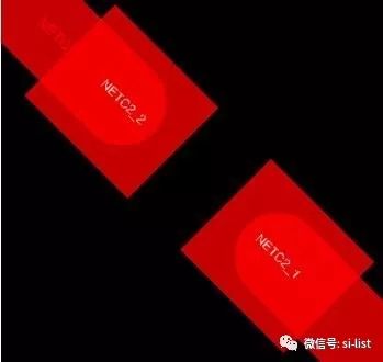
Managing the impedance of inline device and connector pads is also crucial. During inspection, check for gaps or voids in the reference plane around the pads. If there is a noticeable difference between the trace width and the pad size, it could indicate a potential issue.
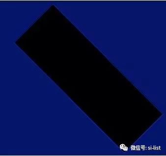
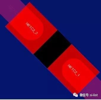
Figure 2 shows a signal trace leading to an inline device, such as a pair of AC-coupling capacitors. Figure 3 displays the ground plane beneath the conductor, showing a notch that helps match the impedance to the transmission line and reduce reflections. Figure 4 presents the top etch and ground plane layout.
Finally, it's essential to run simulations to validate your PCB layout and ensure minimal signal reflections. By following good design practices and applying the guidelines provided, you can significantly reduce simulation time and improve overall performance.
Small Solar Panel
Our Sunket also has a multi-busbar small module production line specializing in the production of small panels for more than ten years.
From 158.75mm 5BB to 182mm 10BB to 210mm 12BB, from 10W to 400W has been fully covered. In addition, our certificates are complete.
Smaller solar panels can be used in many different ways: as a phone charger, for RVs and during camping trips, and for small off-grid solar projects. If you're looking to save money by offsetting your home energy use with a Solar Power System, small panels likely won't get the job done.
Solar panels may be worth it for smaller roofs if you install a system that uses more efficient solar panels, such as monocrystalline solar panels, as they generate more power using less space. The ideal roof slope for solar panels is between 30 degrees and 45 degrees.
Small Solar Panel,Customized Solar Panel,Small Size Solar Panel,Small Size PV Module,Customized PV Module
Wuxi Sunket New Energy Technology Co.,Ltd , https://www.sunketsolar.com