Let's analyze the generation of EMI and ignore the influence of natural interference. In electronic circuit systems, we mainly consider voltage transients and signal reflow.
1 voltage transient
For the analysis of electromagnetic interference, it can be considered from the perspective of electromagnetic energy leakage. If the energy leakage from the device is less, we can think that the electromagnetic interference generated is relatively small. For high-speed digital devices, voltage transients that produce high-frequency AC signals are a major cause of electromagnetic interference. We know that the spectrum generated by the digital signal at the output of the switch is not single, but a lot of higher harmonic components are combined. The amplitude (ie, energy) of these harmonics is determined by the rise or fall time of the device, and the signal rises and falls. The faster the rate, ie the higher the switching frequency, the more energy is generated. Therefore, if the device completes a large voltage transient in a short period of time, it will generate severe electromagnetic radiation, and the leakage of this electromagnetic energy will cause electromagnetic interference problems. In general, the EMI emission bandwidth of high-speed digital circuits can be calculated by the following formula:
F=1/Ï€Tr,
F is the highest EMI frequency generated by the switching circuit in GHz, and Tr is the rise or fall time of the signal in ns.
For example, for a device with a rise time of about 1 ns, the highest EMI frequency it generates will be 350 MHz, and if the rise time is reduced to 500 ps, ​​its highest EMI emission frequency will be 700 MHz, which is much higher than the normal system. The working frequency, which will affect the normal operation of other surrounding systems to some extent.
Obviously, if the rising edge of the signal can be slowed down, EMI will be greatly reduced. However, with the development of electronic design and chip manufacturing, the device is always moving toward high speed. The single signal switching rate is obviously not realistic. But we can achieve the same goal by lowering the signal voltage, because the voltage gate voltage that the low-voltage device needs to cross is small in the same time, which also slows the rising edge rate of the device, so the low-voltage device is also a high-speed circuit. The trend of development.
2 signal reflow
There is a closed-loop loop in the transmission of any signal. When current flows from the driver to the receiver, a return current must flow back from the receiver to the driver through the adjacent conductor to form a closed loop. The size of the loop has a lot to do with the generation of EMI. We all know that each loop can be equivalent to an antenna. The larger the number or area of ​​loops, the stronger the EMI. We know that the AC signal will automatically select the path with the lowest impedance and return it to the driver. However, in reality, the signal cannot always maintain the ideal path as shown in Figure 1, especially on high-density PCB boards, vias, and gaps. Etc. may reduce the ideal characteristics of the reference plane, but rather represent a more complex form of reflow (Figure 2).
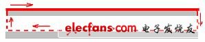
Figure 1 Schematic diagram of ideal signal reflow
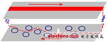
Figure 2 Signal reflow in the actual situation
The understanding of high-frequency signal reflow cannot have a mindset, and it is believed that the reflow must be completely present on the reference plane directly below the signal trace. In fact, the way of signal reflow is multifaceted: the reference plane, adjacent traces, medium, and even air may all be the channels of its choice. Which of the main factors depends on the degree of coupling between them and the signal traces, coupling The strongest will provide the most important return path for the signal. For example, in a multilayer PCB design, the reference plane is very close to the signal layer, coupling most of the electromagnetic field, more than 99% of the signal energy will be concentrated in the nearest reference plane reflow, due to the loop area between the signal and ground return Very small, so the EMI generated is also very low. However, if there is a non-ideal factor such as a gap on the adjacent reference plane, this leads to an increase in the area of ​​the reflow, and the coupling of the low inductance is weakened, and more reflow will be passed through other means or directly released into the air. This will lead to a significant increase in EMI.
We will analyze the effect of signal reflow on EMI with reference to Figure 3. It can be seen that the signal and the recirculating outer region can cancel each other out due to the opposite polarity of the magnetic field, while the middle portion is strengthened, which is also the main source of external radiation. Obviously, as long as we shorten the distance between the signal and the reflow, we can better offset the external electromagnetic field, and at the same time reduce the area of ​​the intermediate reinforcement and greatly suppress EMI.
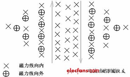
Figure 3 Analysis of the magnetic field coupling of the signal loop
Rice Mill,Rice Mill Machine,Small Rice Milling Machine,Rice Mill Equipment
Hunan Furui Mechanical and Electrical Equipment Manufacturing Co., Ltd. , https://www.thresher.nl