Switching power supplies are now widely used in various terminal and communication devices powered by electronic computers. These power supplies are compact, lightweight, and highly efficient, making them an essential component in the fast-paced development of the electronics and information industry. As microelectronics technology advances, Digital Signal Processors (DSPs) are also evolving rapidly. Their capabilities are becoming more powerful, their cost-performance ratio is improving, and their development methods are continuously being refined. Moreover, DSPs operate 10 to 15 times faster than traditional CPUs. Therefore, switching power supplies based on DSP chips represent a natural evolution, offering great potential for future applications. They can be effectively used in on-board power systems and are expected to become a key trend in the development of switching power supply technology.
**1. PWM Type Switching Power Supply Principle**
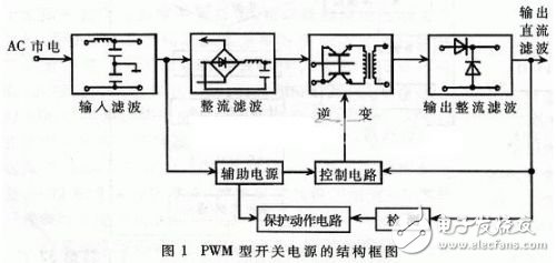
The block diagram of a PWM-type switching power supply is shown in Figure 1. After the AC input is filtered and rectified, it is converted into a smooth DC voltage for the next stage of conversion. The DC is then inverted into AC, which is the core of the PWM control process. Higher frequencies allow for smaller size, lighter weight, and better output performance. Finally, after rectification and filtering, a stable and reliable DC power supply is provided according to the load requirements.
**2. PWM Control Principle**
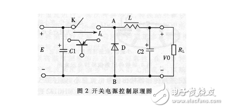
Figure 2 shows the schematic of a switching power supply control system. In this setup, the switch K is turned on and off at regular intervals. When K is on, the power source E delivers energy to the load RL through the switch and filter circuit. To ensure continuous energy delivery, the switching regulator must include energy storage components that store energy when the switch is on and release it when the switch is off. In Figure 2, the inductor L and capacitor C2 serve this purpose. When the switch is off, the stored energy is released to the load via diode D, ensuring a continuous and stable current flow. This is why D is referred to as a freewheeling diode.
The average voltage between points A and B can be expressed as:
EAB = TON / T × E (1)
Where TON is the time the switch is on, and T is the total cycle time (TON + TOFF). By adjusting the duty cycle, the output voltage V0 remains stable even when the input or load changes. This method, known as Time Ratio Control (TRC), involves keeping the switching period T constant while varying the pulse width TON. This technique is called Pulse Width Modulation (PWM), which is used to regulate voltage amplitude and frequency.
**3. Introduction to DSP Chip TMS320LF2407**
The TMS320 series DSP architecture is specifically designed for real-time signal processing. It integrates real-time processing with control peripherals, making it an ideal solution for implementing control systems. The TMS320LF2407, part of the TMS320 family, offers several advanced features:
(a) A high-performance 10-bit ADC with a conversion time of 500ns and up to 16 analog inputs.
(b) A CPU core compatible with the TMS320C2xx family, ensuring code compatibility across the entire DSP range.
(c) Two event manager modules (EVA and EVB), each containing two 16-bit general-purpose timers and eight 16-bit PWM channels.
(d) Up to 24K of FLASH program memory.
(e) Scalable external memory support.
(f) Five external interrupts, including two drive protection, reset, and two maskable interrupts.
**4. Implementing SPWM with TMS320LF2407**
**4.1 Basic Principles of SPWM Control**
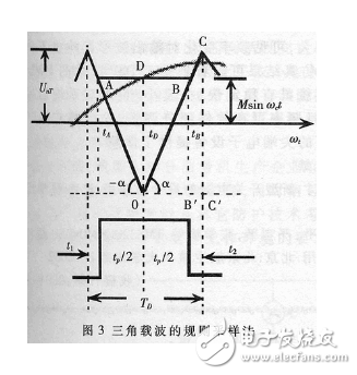
SPWM, or Sinusoidal Pulse Width Modulation, refers to the modulation of pulse widths according to a sine wave pattern. According to sampling theory, narrow pulses with different amplitudes and shapes have similar effects when applied to systems with inertia. To achieve a sine wave output, a series of rectangular pulses with equal amplitudes but varying widths is required. Using the regular sampling method with a triangular carrier, we can generate a rectangular wave whose width follows a sinusoidal pattern. As shown in Figure 3, the midpoint of each pulse corresponds to a point on the triangular wave. At the negative peak of the carrier, a sample point D is taken from the sine wave, and horizontal lines intersect the triangular wave at points A and B. The time interval between tA and tB determines the pulse width.
From the figure, the relationship between AB and the carrier period TC is given by:
AB = TC(1 + sinωctD)/2 (2)
If there are N pulses per cycle, the duty ratio of the first pulse can be calculated accordingly.
**4.2 Implementing SPWM with TMS320LF2407**
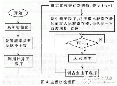
This section illustrates how SPWM control can be implemented using the general timer 3 in EVB and the associated compare unit. By configuring these components, the DSP chip can generate precise PWM signals that follow a sine wave pattern, enabling efficient and accurate control of the switching power supply.
Patch Antenna
The patch antenna, also known as a microstrip antenna, is a type of planar antenna that has found widespread application in modern communication systems due to its low profile, lightweight, and ease of integration with various electronic devices. This article delves into the various classifications of patch antennas, highlighting their unique features and areas of application.
1. Shape Classification
Patch antennas can be categorized based on their shape, which significantly influences their radiation patterns and performance characteristics.
-
Rectangular Patch Antennas: The most common form, rectangular patch antennas offer simple design and fabrication processes. They exhibit a directional radiation pattern with a main beam along the broadside of the antenna.
-
Circular Patch Antennas: Circular patch antennas offer a more omnidirectional radiation pattern, making them suitable for applications requiring broad coverage. They are also visually appealing and can blend seamlessly into various environments.
-
Other Shapes: Innovations in antenna design have led to the development of patch antennas with irregular shapes, such as triangular, hexagonal, and elliptical. These unique shapes can offer customized radiation patterns tailored to specific application requirements.
2. Feeding Mechanism Classification
The method of feeding the antenna, i.e., how the RF signal is coupled to the antenna, is another critical aspect of patch antenna classification.
-
Microstrip Line Feed: In this method, the feedline is placed parallel to the patch and connected to it via a gap or coupling aperture. It offers good impedance matching and ease of integration with microstrip circuits.
-
Coplanar Waveguide Feed: This technique involves placing the feedline in the same plane as the ground plane, simplifying fabrication and reducing cross-talk between adjacent antennas.
-
Aperture-Coupled Feed: Aperture-coupled patch antennas use a slot in the ground plane to couple the feedline to the patch. This method provides better isolation between the feed network and the radiating element, resulting in improved antenna performance.
GSM Patch Antenna,FM AM Patch Antenna,2.4G patch Antenna,4G Patch Antenna,5G Patch Antenna
Yetnorson Antenna Co., Ltd. , https://www.yetnorson.com