0 Preface
This article refers to the address: http://
With the popularity of digital electronic technology, digital signals in the field of broadcasting have gradually replaced traditional analog signals. In recent years, with the popularity of DSP technology and the emergence of high-performance DSP chips, DSP has been increasingly accepted by a large number of engineers, and is increasingly used in speech processing, image processing, pattern recognition and industry. Control and other fields have increasingly shown their great superiority. DSP can use special or general digital signal processing technology to process signals by digital calculation method. It has the advantages of fast processing speed, flexibility, accuracy, strong anti-interference ability, small size and high reliability, which can meet the requirements of fast signal. Accurate, real-time processing and control requirements.
1 ADSP-BF533 chip introduction
The ADSP-BF533 processor is a high-performance product in the Blackfin family that is designed for multimedia (especially video processing) and communications applications. The processor core consists of two 16-bit multipliers (MAC), two 40-bit accumulators, two 40-bit ALUs, four video ALUs, and one 40-bit shifter. The BF533 core operates up to 600MHz and the arithmetic unit can process 8-bit, 16-bit or 32-bit data from the register bank.
The architecture of the Blackfin processor combines the state-of-the-art dual-MAC signal processing engine, the advantages of a compact RISC-based microprocessor instruction set, and single-instruction multi-data (SIMD) multimedia capabilities to form a unique set of instructions. structure.
The processor includes a wide range of peripherals that can be connected to the core via different high-speed broadband buses, making the system flexible and extremely capable. Common peripherals such as UART, timers with PWM (Pulse Width Modulation) and pulse measurement capabilities, general purpose I/O flag pins, and a real-time clock and a "watchdog" timer.
The processor has multiple independent DMA controllers that automate data transfers with minimal processor core overhead. DMA transfers can occur between the internal memory of the ADSP-BF533 processor and any DMA-capable peripherals. In addition, DMA transfers can be done between any DMA-capable peripheral and an external device that is connected to an external memory interface (including SDRAM controllers, asynchronous memory controllers). Peripherals with DMA transfer capabilities include SPORTS, SPI port, UART, and PPI ports. Each individual DMA capable peripheral has at least one dedicated DMA channel.
The BF533 processor has 16 bidirectional general purpose programmable I/O pins (PF15-0). Each programmable pin can be independently controlled by a program flag control register, a flag status register, and a flag interrupt register. Each individual PFx pin provides an interrupt to the processor. Similar to the two flag control registers used to set and clear flags, one flag mask register can be enabled by setting the corresponding bit, and the other flag mask register disables the interrupt function by clearing the corresponding bit. When the PFx pin is defined as an input, it can be set to generate a hardware interrupt; when defined as an output, it can be set to a software interrupt trigger. The flag interrupt sensitive register can be used to specify whether each PFx pin is level or edge sensitive. If it is edge sensitive, it is also specified to be only rising edge sensitive or sensitive to both rising and falling edges of the signal.
The processor provides a full-duplex, universal asynchronous receive/transmit (UART) port that is fully compatible with PC-standard UARTs. The UART port provides a simplified UART interface for other peripherals or hosts to support full-duplex, DMA-capable asynchronous serial data transfers. The UART port supports 5 to 8 data bits, 1 or 2 stop bits, and no parity, odd parity, or even parity bits. The baud rate, serial data format, error code generation and status, and interrupts of the UART port are all programmable.
The processor includes a 32-bit timer that can be used to execute the software's "watchdog" function. The software "watchdog" can improve the reliability of the system. If the timer overflows before the software reset, the software "watchdog" can force the processor to enter by generating a hardware reset, non-maskable interrupt (NMI) or general-purpose interrupt. The person has a known state.
2 system hardware design
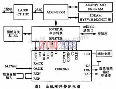
The system is designed with ADSP-BF533 as the core of the audio signal processing system, the main hardware unit is ADSP-BF533, flash, SDRAM, bus interface, and power, clock, JTAG modulator. In addition, there are CPLD chip auxiliary processing. The power module of the system uses TPS70302. The peripheral devices have different RC values ​​to form different voltages. Here, two voltages of 3.3V and 1.2V need to be generated. In addition, there are JTAG debug ports. The hardware block diagram of the entire processor system is shown in Figure 1.
2.1 SDRAM memory
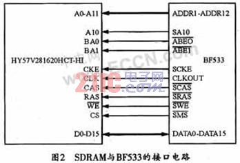
The SDRAM memory is HY57V281620, which has a storage capacity of 4×2 Mx16 bits (16MB) and an operating voltage of 3.3 V. It has a 16-bit data width and can meet storage requirements. The clock of the HY57V281620 is provided by the system clock of the DSP. The data bus D[15:0] is connected to the 16-bit data bus of the DSP. Its interface circuit connection is shown in Figure 2.
2.2 External FLASH
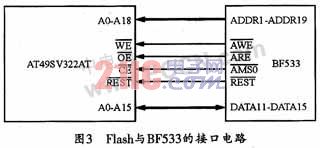
Due to the limited internal storage capacity of the BF-533, FLASH must be externally used for storing programs. The FLASH chip can be used with AT49BV322AT. After each power-on reset, the BF-533 first boots the program in the FLASH to the core. As shown in Figure 3.
2.3 Ethernet chip LAN91C111
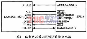
Because the LAN91C111 is a high-speed chip designed according to the general standard timing, and is designed for embedded systems, its peripheral circuit is relatively simple. Figure 4 shows the interface circuit between LAN91C111 and BF533. In the figure, the address buses ADDR0 to ADDR14 of BF533 are connected to LAN91C111 and A1 to A15. A0 is not used by LAN91C111 and is left floating; the data bus is connected to D0~D15 for 16-bit data transmission. D16~D32 of LAN91C111 end are suspended; the chip select signal AEN of LAN91C111 is provided by DSP.
2.4 CPLD section
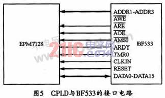
Data communication between the control module and the selected distribution board can be implemented in the CPLD. When the parallel port is switched to the serial port, the BF533 sends 16-bit parallel data to the CPLD every communication. The lower 8 bits are serial port data, and the data can be sent through the trigger. The lower 4 bits of the upper 8 bits are sent to the number distribution board, and the strobe signal is judged thereby, and the serial port data is sent to the corresponding channel at a certain baud rate. When the serial port is turned to the parallel port, the corresponding baud rate clock is first simulated, and the pin is sampled by this clock. When the serial port start bit is detected, the sampling data is stored, and the data and channel status are sent to the BF533. Pins connected to the parallel port. After that, the pin connected to the PF of the BF533 is set to cause the BF533 to be interrupted and the parallel port data is read. In this way, the data transmission and reception of the 10-way asynchronous serial port can be controlled through the parallel data bus of the DSP. The EPM7160 uses a 24.576 NHz crystal input and internally divides the input clock by programming according to the baud rate of the external serial port. Its CPLD interface circuit connection is shown in Figure 5.
3 system software design
The Blackfin family of DSPs supports both C and assembly language in software, while supporting mixed programming of both. C language program structure is good, readable, easy to transplant, but the processing speed is slow. Assembly language processing is fast, but it is poorly readable and not easy to debug. The mixed programming of C language and assembly language can combine their respective advantages and can construct a program with good structure and fast execution speed. But in the programming process should pay attention to the following matters: First, whether in C or assembly language, there is only one set of the same register available in the system, so before using the register, the subfunction must be saved first, and before returning restore. Second, it must be used strictly in accordance with the type of register. Different types of registers cannot be mixed. Third, in order to improve the speed of the code, you should be good at using parallel instructions.
After the system initializes the BF533 program, the main program will accept the parsed audio signal sent by the SPORT port at any time, and store the corresponding maximum level value, and simultaneously turn on the UART interrupt and the TIMER0 interrupt. In the TIMER0 interrupt (this system is initially set to 10 ms), the stored data can be processed and the status extracted. If the requirement is not met, the TIMER1 interrupt is turned on (the system is initialized to 6 s), and jumps back to the main program to continue the test. If the corresponding TIMER1 interrupt does not meet the requirements, the switch is performed. The UART interrupt completes the data exchange with the control board and the host computer.
In each program module, the main program module main() mainly completes the initialization work of the system and various interfaces, detects the recording level, monitors the state, waits for the interrupt to occur, etc., wherein the Timer0 interrupt subroutine module EX_INTERRUPT_HANDLER (Timer0_ISR) can complete the storage. The data is processed and the status function is extracted. The Timer1 interrupt subroutine module EX_INTERRUPT_HANDLER (Timerl_ISR) can complete the level detection to determine whether to switch during the set delay. The asynchronous serial port interrupt subroutine module EX_INTERRUPT_HANDLER (Uart_ISR) is used to complete the receiving host computer and board signal control functions.
4 Conclusion
ADI's BF533 can be used to process new signals and expand SDRAM as a large-capacity memory. The system has low cost, high efficiency, good real-time performance and excellent performance.
Landscape Lamp lighting is decorative light source configuration of city garden landscape,cultural and recreational square and large-scale social activities widely used and essential,is a decorative lighting products.Rod material diverse use of flexible,light,sound,light,electricity three-in-one,structure and morphology in different poses and with different expressions,beautify,lighting,green organic combination,light and shadow,perfect crystal lamp and art.


1. Decorative landscape lighting products.Design style or abstract avant-garde such as artistic sculpture, or simulation realism such as natural normal elements can beautify the lighting environment and become a symbol of the national culture in a city.Whether it is a large cultural square or a fashion building community, there is a reason for it.Excellent viewing and use value.
2. applicable place:Park, courtyard and upscale residential area, road side, commercial pedestrian street, leisure plaza, scenic tourist area, etc.
3. material description:Steel lamp body, the whole high quality hot dip galvanizing after electrostatic spraying, not rusting, aging, surface clean.The light source is metal halide lamp, energy-saving lamp and LED.
Landscape Lamp
Landscape Lamp,Landscape Lamp Post,Landscape Lampshade,Landscape Lamps
Jiangsu chengxu Electric Group Co., Ltd , http://www.satislighting.com