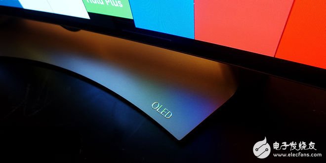
Taiwan's DigiTImes news said that according to Apple's source of information in Taiwan's supply chain, Apple's iPhone, introduced 1-2 years later, may use a 5.8-inch OLED screen. That is, iPhones in 2017 or 2018 may use OLED screens.
If you have a little understanding of the display, you must know that the iPhone has been using the LCD screen since its inception. The star of the OLED screen on mobile phones is actually starting from Samsung's Galaxy S generation in 2010. Compared with the LCD screen, the OLED screen has a wider color gamut, and the contrast is higher than the LCD.
However, at the same time, the application of OLED screens in mobile phone products has always had the reputation of being too bright, low in brightness, color cast, and even grainy. However, since last year's Galaxy S6, Samsung's OLED screen has the ability to compete with mainstream LCDs in terms of color registration and brightness. At the same time, color gamut and contrast remain absolutely dominant. In addition, from the structural point of view, OLED screen is more conducive to thin and flexible, curved structure, it is not difficult to understand Apple's future decision to focus on OLED screen.
However, in the field of large-screen TVs and displays, the price of products using OLED panels is still high, which is closely related to the technical difficulty and low yield of OLED panels, resulting in higher costs. It seems that OLED screens are replacing LCD screens in the mobile phone industry, but in the big screen market, it seems that they have to spend a lot of effort.
Fortunately, there are still many companies working hard for OLEDs. From the process, it is the way out for OLEDs to break through. This time we prepared a long article for students who are looking to learn more about the technical details of OLED. Let's talk briefly about one component of the OLED manufacturing process: evaporation. And how vendors like Panasonic can make further cost savings in this part of the process, and how Sony has improved this step.
do you know? Each pixel "bulb" of the OLED screen is steamed up.
Continuing the rumors that the related iPhone 8 may adopt an OLED screen. South Korean media ET News mentioned at the end of last month that Samsung may become Apple's largest OLED panel supplier on the new iPhone, followed by LG, Sharp, etc. Samsung may account for 5-8% of the orders. Share.
The news also mentioned that LG may not be the second largest supplier because LG's evaporation device is not enough, so OLED panel production can not meet Apple's needs. The meaning is roughly that Samsung's vaporizers are sufficient - Samsung's vaporizers are certainly not made by themselves. The next supplier is Canon Tokki - yes, this is a subsidiary of Canon. . So perhaps in the future iPhone 8, Canon Tokki's vaporizer will play a vital role.
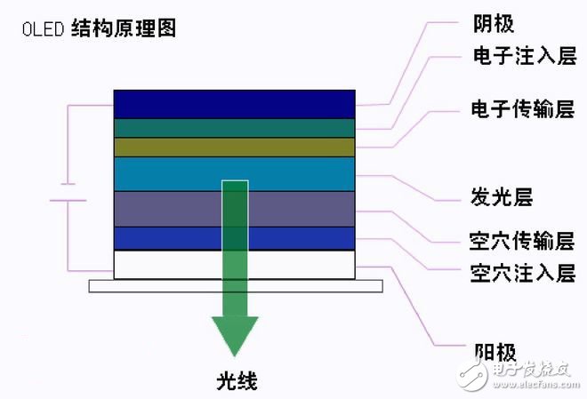
So what exactly is evaporation? This has to start with the structure of OLED. As shown in the above figure, the typical structure is to make a layer of tens of nanometers thick luminescent material on ITO glass - that is, people usually say OLED screen pixel self-luminous material, there is a layer of metal electrode above the luminescent layer, the electrode is applied with voltage, and the illuminating The layer generates light radiation; electrons and holes are injected from the yin and yang respectively, and the injected electrons and holes are transported in the organic layer, and are combined in the light-emitting layer to excite the light-emitting layer molecules to generate singlet excitons, and the singlet exciton radiation is attenuated. Glowing.
This is a bit more complicated to explain, but in general, the three sub-pixels you see, red, green and blue will shine on your own. Of course, the structure is much more complicated when it comes to the entire panel, including isolation columns, insulation layers, and the like between sub-pixels. AMOLED also has a TFT backplane that controls each pixel switch.
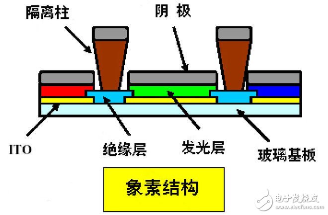
This complicated structure is impossible to use for a micro-carving with a knife. If these structures are put into practice, it is a problem with the manufacturing process. The manufacturing process of OLED involves ITO glass cleaning, lithography processing, etc., all of which require high-tech, technologies that we have never seen before. In short, ITO can form electrode patterns and ITO on the substrate. Patterns, isolation column patterns, etc. - you can imagine that there are small people carved with a knife...
Subsequent process parts are crucial in the manufacture of OLED panels, namely evaporation. Inside the vacuum chamber, place the ITO glass substrate on a heated rotating sample holder, then put the fire under it (of course not really put the fire), and the luminescent material you see is steamed up. Yes, the red, green and blue tri-color bulbs (of course not the real ones) are steamed up.
Speaking taller, evaporation is the process of heating in the vacuum, electron beam bombardment heating and laser heating to evaporate the vaporized material into atoms or molecules, which then move in a straight line with a large free path, colliding the substrate. The surface is condensed to form a film.
It can be said that evaporation is the essence of the OLED manufacturing process, and not only luminescent materials, metal electrodes and the like are also steamed up. Although we have the same evaporation method as steamed steamed buns, the actual operation is very complicated, such as how to control the pixel area, how to align the pixels, and how to control the thickness of the film that is steamed up, what pretreatment, and the vacuum degree of the evaporation chamber. Wait, it is not something that most of us can penetrate. In addition to evaporation, there are subsequent processes such as dispensing, encapsulation, aging, cutting, testing, and the like.
In fact, evaporation is indeed an important reason for the high cost of OLED screens, so LG can't buy too many evaporation machines, and naturally it can't make an order for iPhone 8. And even Canon Tokki, it is not easy to digest Samsung's orders.
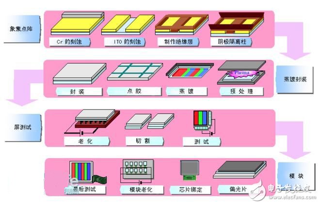
(This is a typical process flow of PMOLED, PMOLED is also an OLED, but the structure is simpler than AMOLED, no TFT)
Multifunctional High Speed Blender,Mute Wall High Speed Blenders,Household High-Speed Blender,Good High Speed Blender
JOYOUNG COMPANY LIMITED , https://www.globaljoyoung.com