1 Introduction
This article refers to the address: http://
High-speed and large-capacity image data acquisition and display systems have broad application prospects in radar, meteorology, earthquake prediction, aerospace, communications and other fields. The signal processing in these fields has the characteristics of strong real-time performance, high data rate, large amount of data, complicated processing and large amount of calculation. This requires image data acquisition to have the ability to process large amounts of data; and is rigorous in terms of size, power consumption, and stability. A high conversion rate, low power A/D converter combined with an efficient FPGA can fulfill this functional requirement. Since the image display interface uses different USB control processing devices, the host needs to install various dedicated drivers and is incompatible with each other. Therefore, it is necessary to provide a unified data exchange specification to the video device of the USB interface to conveniently and quickly communicate with the computer. Therefore, a solution based on the AD9883A and USB VGA image acquisition and display system is given here.
2 system overall design
Figure 1 is a block diagram of an image acquisition and display system.
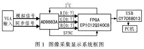
(1) The VGA input module inputs the analog signal RGB and the line sync signal, and the field sync signal to the A/D conversion module. Since the module is composed of analog circuits and is prone to noise, the interface device should be placed as close as possible to the A/D converter.
(2) The A/D conversion module first determines the sampled horizontal and vertical frequency according to the synchronization signal, and then determines the pixel clock by the horizontal frequency and the internal register, and the internal PLL of the A/D converter generates the pixel clock. The analog signal input from the VGA is converted into an 8×3 digital video signal, and the sampling effect of the image is adjusted through a series of registers.
(3) FPGA control module On the one hand, the FPGA writes control information to the A/D converter register through the I2C bus; on the other hand, it outputs 8×3 digital signals. When the FPGA receives 8×3 signals, its pixel frequency is 75 MHz, which is inconsistent with the internal clock frequency of the FPGA, and the data rate is large. Therefore, the two FIFOs can be read by pingpong.
(4) USB output display module FIFO is an asynchronous interface with data buffering function. The data stored in the FIFO is acquired by the USB controller and transmitted to the computer through the USB interface for display.
3 system hardware design
3.1 VGA interface
VGA is a D-type interface that can transmit VGA, SVGA, XGA, SXGA and other image formats. The VGA interface has a total of 15 pins, divided into 3 rows, 5 in each row. The VGA interface is the most widely used interface type for graphics cards.
The system VGA analog signal input is connected to the A/D converter, and the RAIN, GAIN, and BAIN of the A/D converter are respectively connected to the R, G, and B of the analog interface.
3.2 A/D conversion interface
Since the sampling rate of the A/D converter is high, the corresponding output data rate is also high. At the highest system requirements, the pixel frequency is 108 MHz and the corresponding data rate is 324 Mbit/s (R, G, B 3 components, 8 bits each). At the same time, due to the acquisition of image data, higher line synchronization is required. If one line of image data loses one or more points of data, the entire image will be skewed. Therefore, each row of data needs to be stored in a burst to ensure that the data is not lost. Its burst length is the horizontal resolution of the image.
The A/D converter of this acquisition module uses the AD9883A. The device is specifically designed to acquire analog R, G, and B signals and digitize them for display or for other applications. The device has a 3-channel channel with a sampling accuracy of 8 bits, a maximum sampling rate of 140 MS/s, 300 MB of analog bandwidth, and an optimized image interface for computers and workstations with a sample resolution of 1280×1024. A video signal with a refresh rate of 75 Hz. The AD9883A-based circuit provides a good computer interface for high-definition television (HDTV) and a front-end scan converter for high-performance video equipment. The internal structure of the AD9883A is shown in Figure 2.
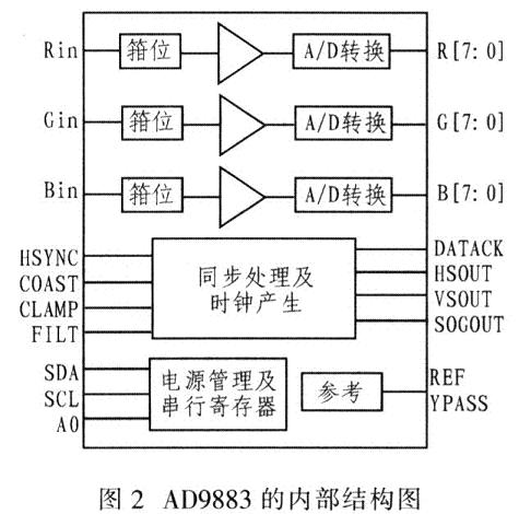
After inputting the VGA image signal, clamp it first to adjust its DC offset component so that the input level meets the A/D conversion module requirements. The AD9883A has three high-bandwidth, 8-bit resolution, 110MS/s slew rate A/D converters. It samples, quantizes, and encodes the clamped analog video signal to obtain a digital video signal. , get the best conversion effect.
The sampling clock is generated by configuring a phase-locked loop (PLL). The line sync signal (HSYNC) can be used as a reference clock and then divided to obtain the sampling clock required by the A/D converter. The AD9883A integrates an ultra-low jitter phase-locked loop that oscillates less than 5% of the clock in all modes of operation. The stability of the AD9883A clock is important for the system to produce clear and stable images. Because the AD9883A has a wide range of adjustable phase-locked loops that can produce pixel frequencies from 12 to 140 MHz, the AD9883A supports a rich input image format.
The AD9883A's sync signal generation module can recognize a variety of sync signal input modes, and can also flexibly set the sync signal output mode as needed. Device initialization is facilitated by I2C bus timing.
The A/D conversion module can collect multiple VGA image formats, but it cannot automatically detect the image format. It must be set by the I2C interface provided by it. The FPGA automatically detects the image format and sets the A/D conversion module. In addition, the effective pulse level of the field sync signal in different formats of VGA images is not uniform, and the A/D conversion module can automatically detect the polarity of the input field sync signal and store it in an internal register, and read the register to determine the input VGA signal field. The polarity of the synchronization. The field sync signal output by the A/D conversion module implements the inversion of the input field sync signal. The internal synchronization logic of FP-GA only supports an active level field sync signal. Therefore, the A/D converter internal register needs to be read before the acquisition to determine the polarity of the current input sync signal to determine whether A/ needs to be set. The D converter inverts the field sync signal.
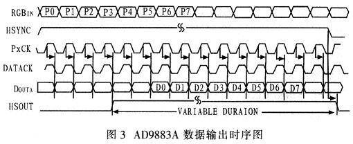
After the input analog video signal is clamped, gain and bias controlled, the three high-precision high-speed A/D converters in the AD9883 are converted to the digital video signals required for display by the sampling clock generated by the phase-locked loop. Figure 3 shows the timing of its data output. On the falling edge of the output data clock DATACK, the corresponding signal is sampled and quantized. The quantized data is output on the rising edge of the clock: the interface circuit accurately latches the image data with the rising edge of DATACK. Digital image acquisition. Considering the pixel clock and the phase delay of the data, HSYNC can be used to eliminate the uncertainty of the edge timing. It should be noted that the AD9883A has a data output channel that must be cleared before the output data is valid, resulting in the output of 4 sets of invalid data before each line of valid data is output. This invalid data can be avoided by counting the clock.
3.3 FPGA Controller Design
The master FPGA generates the control signals required by the system to ensure that each module works together. The system is designed using the EP1C12Q240C8 FPGA. Its internal module block diagram is shown in Figure 4.
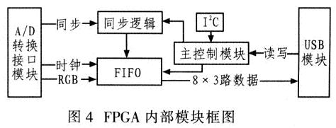
The FPGA is composed of main control, A/D conversion interface, FIFO, and USB. The main control module is responsible for coordinating the work between the modules. The A/D conversion interface module receives the data and synchronization signals output by the A/D conversion module and ensures the line and field synchronization of the image data. The FIFO module uses the pingpong method to read the 8×3 digital signals transmitted by the A/D conversion, and then The USB output interface module outputs high speed data.
3.4 Output display design
The USB interface module provides a reliable interface for applications and functional devices. The USB system can be divided into two parts: a USB host and a USB device. The block diagram of the module is shown in Figure 5.
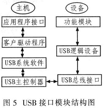
The USB interface device uses Cypress's EZ-USB FX2 device CY7C68013A. The device integrates USB 2.0 transceiver intelligent serial engine SIE, enhanced 8051 controller, general purpose programmable interface (GPIF), 8.5 KB RAM and 4 KB FIFO memory. The original design of FX2 series can meet USB2. Bus bandwidth of .0.
The system is mainly based on transmission control information and video data. The device can be placed in the Slave FIFO mode. The USB serial interface engine (SIE) directly transmits data to the Slave FIFO, and the Slave FIFO communicates with an external device (FPGA) to implement the PC. The machine communicates with the FPGA and displays the video data.
3.5 USB device driver development
The USB device driver mocks the bridge between the USB peripherals, the operating system, and the user application, and is the software interface that connects the USB device to the computer system. There are two kinds of device drivers for EZ-USB FX2 device CY7C68013A: one is used to download the firmware storage RAM from the host when the device is connected, which is called the same download driver (wdgtldr.sys); the other is The device re-enumerates the generic device driver (ezusb.sys) that is loaded, and the application software communicates with FX2 through the device driver. Write a class USB Video Class of the host computer program, which corresponds to the same piece of hardware CY7C68013A. The purpose of the Video Class protocol is to provide a unified data exchange specification for the video device of the USB interface, so that CY7C68013A does not need ezusb after accessing the PC. Sys, but use the PC's own Video driver to identify it as a Video device.
The program code of the firmware can be downloaded from the external E2PROM or downloaded from the host. It is downloaded from the host. Among them, the USB Video Class protocol is that the host side obtains the structure of the video device side and the functions supported by the device by acquiring a descriptor (Descriptor). To control these function modules and configure the data source and data flow, you need to complete the Request (including the Standard Device Requests and Class and related Class Specific Requests that all USB devices need to support).
The operating system supports Video Class through a driver. The overall framework of the Video Class driver is divided into two parts: one is responsible for processing the initialization of the module, handling the interaction of Descriptor and Requests on the USB bus, including the control, query, reception, interpretation, and response of the USB bus: another part Is a separate kernel thread that is started in initialization. Responsible for executing specific control commands to acquire and transfer image data.
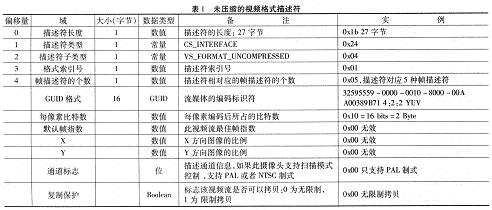
Table 1 shows the definitions and examples of the Uncompressed Video Format Descriptor in the USB Video Class program. This descriptor defines the characteristics of a particular video stream that defines the information for unreduced video, including all YUV types. A video terminal contains a USB endpoint IN or OUT belonging to the associated channel and supports one or more format definitions. In order to select a specific format, the host needs to send a control request to the relevant channel.
4 Conclusion
Realize 8×3 bit based on AD9883A and USB, high speed image data sampling and display system design. The system has a maximum sampling rate of 110 Ms/s. The high-speed and low-power AD9883A samples 1024×768 and 70Hz images. Through the FPGA control circuit, CY7C68013A is used as a dedicated interface device for USB2.0 to realize PC and PFGA. The communication uses the USB Video Class class without loading additional generic device drivers. Using a high-speed A/D converter, FPGA and USB work together to achieve high-speed and integrated circuits. The system can be widely used for real-time recording of image data in radar, weather forecasting, aerospace, communications and other fields.
Front Door Locks,Sliding Door Lock,Security Door Locks,Bedroom Door Lock
YONGFA INTELLIGENT TECHNOLOGY SECURITY CO., LTD. , http://www.yongfa-safe.com