For high-precision test equipment like vector network analyzers, expensive mechanical switches are often the best choice. However, in mass-produced consumer devices such as CATV or SATV systems, cost-effective electronic switches are more suitable. These switches typically use transistors or PIN diodes. Unlike mechanical switches, semiconductor-based switches have no moving parts, which gives them faster response times and a longer operational lifespan.
PIN diodes are widely used in SPST and SPMT switching configurations. They function as variable resistors for signals above ten times their cutoff frequency (fc). When forward-biased, the junction resistance (Rj) of the PIN diode can be adjusted from a high impedance to a low resistance state. This makes them versatile for both series and parallel switching modes.
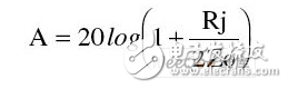
In series mode, the insertion loss is given by:
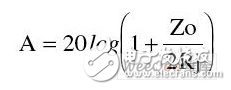
When connected in parallel, the insertion loss becomes:
Here, Zo represents the characteristic impedance, commonly 50 or 75 Ω in RF systems.
The design of a selector switch involves balancing bandwidth and isolation. Series switches offer low insertion loss over a wide frequency range but provide less isolation. Parallel switches, on the other hand, are often used with quarter-wave transmission lines, which limit the bandwidth but offer better isolation.
Both test instruments and CATV/SATV systems require RF switches that operate across multiple octaves with minimal signal loss. In multi-carrier environments, linearity is crucial to avoid inter-channel interference and signal degradation caused by distortion.
To enhance isolation, multiple PIN diodes can be connected in series. This configuration allows shared bias current, reducing power consumption. The ability to cascade PIN diodes makes them more flexible compared to three-terminal transistors, which require separate control circuits for each additional component.
Body-effect diode vs. epitaxial growth type PIN diode
Designers must understand the differences between body-effect and epitaxial (Epi) PIN diodes, as they significantly impact RF performance and application suitability. Body-effect diodes have a low doping density and require higher bias currents. This makes them unsuitable for battery-powered devices. Their thick intrinsic layer results in long carrier lifetimes (300–3,000 ns), which helps maintain low distortion in switches and attenuators.
In contrast, Epi diodes have a highly doped intrinsic layer and are ideal for low-current applications. However, their shorter carrier lifetime (5–300 ns) leads to worse linearity, making them unsuitable for attenuator applications, especially at low bias currents.
The operating frequency range of a PIN switch is influenced by its cutoff frequency. Below 10 times fc, the diode behaves unpredictably, switching between inductive and capacitive characteristics. At even lower frequencies, it acts like a traditional PN junction. Body-effect diodes generally support lower frequencies due to their thicker I-layer.
PIN diode model
Parasitic components such as inductors and capacitors in the diode package affect switching performance. In series configurations, package capacitance and junction capacitance cause isolation to decrease with frequency. Parasitic inductance increases insertion loss at higher frequencies. To improve microwave performance, manufacturers are developing smaller packages with fewer parasitic elements. Standard plastic packages like SOT323, SOD-323, and SOD-523 reflect this trend.
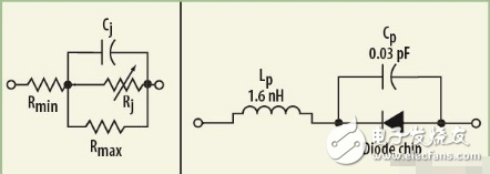
Unfortunately, standard SPICE models do not account for the minority carrier lifetime parameter essential for PIN diodes. A simplified linear model consisting of two resistors, a variable resistor, and a capacitor can represent the chip, as shown in Figure 1.
ZHOUSHAN JIAERLING METER CO.,LTD , https://www.zsjrlmeter.com