LED (Light-Emitting Diode, abbreviated LED) is the abbreviation of LED. Since the second half of 2009, the LED market has made a big leap. As a high-growth emerging industry, it is expected that by 2015, the LED industry will exceed 500 billion yuan. Among them, the general lighting industry is 160 billion yuan, the large-size LCD TV backlight industry is 120 billion yuan, the automotive lighting industry is 20 billion yuan, the general lighting industry is 160 billion yuan, and the landscape, display and other industries are 100 billion yuan.
The LED industry chain can be roughly divided into three parts, namely, upstream substrate growth, epitaxial wafer manufacturing, midstream chip packaging and downstream application products. In the entire industrial chain, the core part is in the process of substrate growth and epitaxial wafer manufacturing. The technical content of the two is relatively high, accounting for nearly 70% of the industry's output value and profits.
At present, due to the influence of international and domestic markets, China's LED industry has initially formed a substrate material including LED upstream, production of LED epitaxial wafers , and preparation of LED chips under the promotion of “National Semiconductor Lighting Projectâ€. The LED chip package and the relatively complete industrial chain of LED products .
It is well known that semiconductor light-emitting diodes have the advantages of high conversion efficiency and long life, and are considered as the next-generation light source and will replace the conventional light source currently used. However, in view of the performance of LEDs, there are still many technical difficulties to be overcome to achieve this goal. It is necessary to increase research efforts in material analysis and device analysis techniques. Optical microscope, scanning electron microscope, X-ray energy spectrum, secondary ion mass spectrometer and other equipment become the device failure and structural analysis in the package structure of the LED device and the analysis of the structure, composition and interface condition of the chip. Monitor, improve and enhance the essential analytical tools.
The following section will briefly introduce some of the applications of Zeiss's optical microscopes and scanning electron microscopes in the production of LEDs.
First, the specific application of Zeiss optical microscope and scanning electron microscope in the upstream substrate material of LED (sapphire material):
1. Introduction of sapphire substrate material
Because sapphire has good insulation, low dielectric loss, high temperature resistance and corrosion resistance. Good thermal conductivity and high mechanical strength. And can be processed into a flat surface. The light transmission band is wide. Therefore, it is widely used in many fields of industry, national defense and scientific research. It is also a good substrate material for a wide range of light-emitting diodes. The resulting light-emitting diodes are the most promising semiconductor illuminator substrate materials for the next generation of fluorescent lamp sources in sapphire substrate substrates in the high-brightness LED family. At present, these high-brightness light-emitting diodes have been widely used in advertising, Traffic Lights, instrument lights, and surgical lights. With the increasing use of high brightness LEDs.
LED sapphire (Sapphire) is a single crystal of alumina, also known as corundum. Sapphire crystal has excellent optical properties, mechanical properties and chemical stability. It has high strength, high hardness and erosion resistance. It can work under the harsh conditions of high temperature close to 2000 °C. According to research, there are only four kinds of substrate materials that can be applied to LEDs. As an important technical crystal, sapphire has formed a more fashionable and mature application in the LED industry.
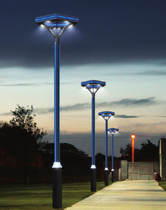
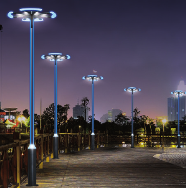
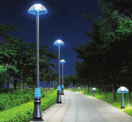
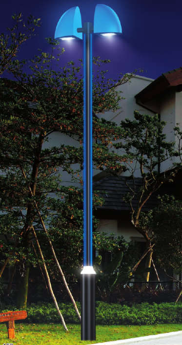
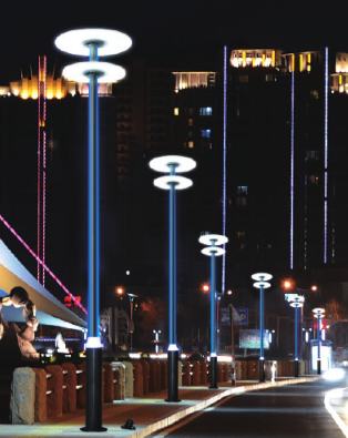
Garden Lamp is a kind of outdoor lighting lamps and lanterns, usually refers to the outdoor Road Lighting lamps and lanterns below 6 meters.The Garden Lamp is characterized by its diversity, beauty and decoration environment, so it is also called landscape courtyard lamp.Slow lane, narrow lanes and is mainly used in city residential areas, tourism scenic area, outdoor lighting, park, plaza and other public venues can prolong people's outdoor activities, improve the security of the property.
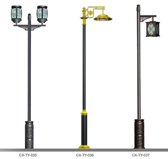
The Garden Lamp has many styles, each style has its own unique name.For example, Water,Moon,Diamonds,Lucky and UFO, these garden lights are not only elegant in name, but also artistic and elegant in appearance.
The Garden Lamp body is aluminium alloy profile is used for manufacturing, high strength, light pole electrostatic powder spraying process, anti graffiti proof, radiation stainless steel links, anti-corrosion ability, patent luminous light pole, the built-in LED light source, disassembling design is reasonable, easy to install and maintain, installation height is 3 to 5 meters.
Technical parameters
|
Chip |
CREE/SAMSUNG/PHLIPS |
|
Initial luminous flux |
≥90LM |
|
Color temperature |
3800-6000K |
|
Level of protection |
IP65 |
|
Power factor |
0.96 |
Garden Lamp
Garden Lamp,Garden Lamp Post,Garden Lamps Solar,Garden Lamp Post Solar
Jiangsu chengxu Electric Group Co., Ltd , https://www.satislighting.com