Integrated DC logarithmic amplifier
Abstract: In the application of logarithmic amplifiers, DC logarithmic amplifiers still occupy a dominant position in the application of compressing the dynamic range of sensor signals, which is a cost-effective solution. This paper derives the transfer function of the DC log amp, from the VBE of bipolar transistors to the IC characteristics. The circuit structure of the integrated DC logarithmic amplifier and the effects of various errors on the logarithmic performance are discussed, and the MAX4206 design example is given. Finally, the method and design details for improving the performance of the log amplifier through calibration are also given.
For more than half a century, engineers have used logarithmic amplifiers to compress signals and perform calculations. Although almost all digital ICs have replaced logarithmic amplifiers in computing applications, engineers still use logarithmic amplifiers for signal compression. Therefore, logarithmic amplifiers are still a key component in many video, fiber, medical, test, and wireless systems.
As the name implies, the relationship between the output and input of the logarithmic amplifier is a logarithmic function (due to corresponding different bases, there is only a constant coefficient difference between the logarithmic functions, so the logarithmic base is not important). Using a logarithmic function, you can compress the dynamic range of the system signal. Compressing signals with a wide dynamic range has many advantages. The combination of logarithmic amplifiers and low-resolution ADCs can usually save board space and reduce system cost. Otherwise, a high-resolution ADC may be required. Moreover, usually the current system already contains a low-resolution ADC, or the microcontroller has such an ADC built in. Converting to logarithmic parameters is also beneficial for many practical applications, such as applications that express measurement results in decibels, or sensor applications whose conversion characteristics are exponential or near-exponential.
In the 1990s, the field of optical fiber communications began to use logarithmic amplifier circuits to measure the optical signal strength in certain optical applications. Prior to this, precision logarithmic amplifier ICs were not only costly, but also bulky; only a few electronic systems could afford such high costs. The only alternative to these IC solutions is to build a logarithmic amplifier using discrete components. Constructing a logarithmic amplifier from discrete components not only has a larger circuit board area, but also is usually sensitive to temperature changes, and must be carefully designed and laid out. It also requires a high degree of matching between the constituent elements in order to ensure good performance over a wide range of input signals. Since then, semiconductor manufacturers have developed smaller, lower-priced integrated logarithmic amplifier products with better temperature characteristics and more functions.
Logarithmic amplifiers are mainly divided into 3 categories. The first type is the DC logarithmic amplifier, which generally handles DC signals that change slowly, and the bandwidth can reach 1MHz. Undoubtedly, the most common implementation is to use the inherent logarithmic IV transmission characteristics of pn junctions. These DC logarithmic amplifiers use unipolar input (current or voltage), usually referring to diodes, transdiodes, linear transconductance and transimpedance logarithmic amplifiers. Because of the current input, DC logarithmic amplifiers are usually used to monitor the current-value or proportional value of a unipolar photodiode with a wide dynamic range. Not only does fiber optic communication equipment require photodiode current monitoring, it can also be found in chemical and biological sample processing equipment. There are also other types of DC logarithmic amplifiers, such as logarithmic amplifiers based on the time-voltage logarithmic relationship of the RC circuit. However, such circuits are generally more complex, have a greater difference from each other, resolution and conversion time are related to the signal, and are more sensitive to temperature changes.
The second type of logarithmic amplifier is a baseband logarithmic amplifier. This type of circuit handles rapidly changing baseband signals and is suitable for applications that require compression of AC signals (usually certain audio and video circuits). The output of the amplifier is proportional to the logarithm of the instantaneous input signal. A special baseband logarithmic amplifier is a "true logarithmic amplifier", which inputs a bipolar signal and outputs a compressed voltage signal consistent with the input polarity. True logarithmic amplifiers can be used for dynamic range compression, such as RF IF level and medical ultrasound receiver circuits.
The last type of logarithmic amplifier is a demodulated logarithmic amplifier, or a continuous detection logarithmic amplifier. This type of logarithmic amplifier compresses and demodulates the RF signal and outputs the logarithm of the envelope of the rectified signal. RF transceivers generally use demodulated logarithmic amplifiers to control the output power of the transmitter by measuring the strength of the received RF signal.
In a typical DC logarithmic amplifier based on a pn junction, a bipolar transistor is used to generate a logarithmic IV relationship. As shown in Figure 1, the feedback path of the operational amplifier uses a transistor (BJT). Depending on the type of transistor selected (npn or pnp), the logarithmic amplifier is a current sink or current source type (Figures 1a and 1b). Using negative feedback, the op amp can provide enough output voltage for the base-emitter junction of the BJT to ensure that all input current is drawn by the collector of the device. Note that the floating diode scheme will cause the equivalent input offset in the output voltage of the op amp; the method of grounding the base will not have this problem. 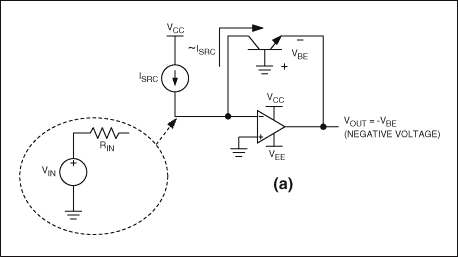
Figure 1a. Basic BJT implementation of a DC logarithmic amplifier, with current sink input, producing a negative output voltage 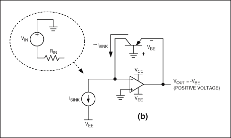
Figure 1b. Change the BJT from npn type to pnp type, the logarithmic amplifier becomes a current source circuit, and the output is positive.
After increasing the input series resistance, the DC logarithmic amplifier can also use voltage input. Using the virtual ground of the operational amplifier as a reference terminal, the input voltage is converted into a proportional current through a resistor. Obviously, the input offset of the operational amplifier must be as small as possible to achieve accurate voltage-current conversion. The implementation of bipolar transistors is sensitive to temperature changes, but the use of reference current and on-chip temperature compensation can significantly reduce this sensitivity, which will be discussed below.
In the circuit shown in Figure 2, the BJT logarithmic amplifier has two inputs: IIN and IREF. As mentioned in the previous section, the current input to IIN causes the op amp A1 to output the corresponding voltage: 
among them:
k = 1.381 x 10⁻²³ J / ° K
T = absolute temperature (° K)
q = 1.602 x 10⁻¹⁹ ° C
IC = collector current (mA or the same unit as IIN and IS)
IIN = logarithmic amplifier input current (mA or the same unit as IC and IS)
IS = reverse saturation current (mA or the same unit as IIN and IC)
(In Equation 1, "ln" represents the natural logarithm. In the following equation, "Log10" represents the logarithm to the base 10). 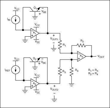
Figure 2. Using two basic BJT input structures and subtracting VOUT2 from VOUT1 eliminates the temperature effect of IS at the output. The remaining "PTAT" effect can be minimized by selecting the appropriate RTD (resistance temperature probe) and gain setting resistance of the differential amplifier.
Although this expression clearly shows the logarithmic relationship between VOUT1 and IIN, the IS and kT / q terms are related to temperature and will cause a large change in the VBE voltage. To eliminate the temperature effect caused by IS, a differential circuit is formed by A3 and its peripheral resistors, and the second junction voltage is subtracted from VOUT1. The second junction voltage is generated in a similar way to VOUT1, except that the input current is IREF. The characteristics of the transistor providing the two junctions must be very consistent, and the temperature environment must also be very close to achieve the correct cancellation function. 
The adoption of IREF brings two benefits. First, it can set the required x-axis "logarithmic intercept" current-the current that makes the logarithmic amplifier output current theoretically equal to zero. Second, in addition to absolute measurements, it also allows users to make proportional measurements. Ratio measurement is usually used in optical sensors and systems. In such systems, the attenuated light source needs to be compared with the reference light source.
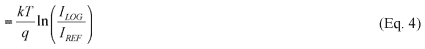
Equation 5 still has a temperature effect, VDIFF is proportional to absolute temperature (PTAT). By adding a subsequent temperature compensation circuit (usually an operational amplifier stage with a resistance temperature detector (RTD), or similar device, which is also part of the gain configuration), it can effectively eliminate PTAT errors and produce an ideal logarithmic amplification relationship: 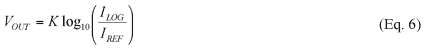
Among them, K is a new proportional constant, also known as logarithmic amplifier gain, expressed in V / 10 octave. Since the ratio ILOG / IREF using log10 operation determines that ILOG is greater than or less than 10 times the number of IREFs, multiplying by K will produce the required voltage unit.
The DC logarithmic amplifier is very suitable for the use of integrated design schemes, because key temperature-sensitive components can be placed together in the circuit to facilitate tracking the temperature changes of these components. Moreover, in the production process, it is also easy to fine-tune various residual errors. Various residual error indicators will be explained in detail in the data file of the logarithmic amplifier.
The functional block diagram shown in Figure 3 shows the structure of a typical contemporary DC log amp (MAX4206). Similar to previous amplifiers, today's DC logarithmic amplifiers also use operational amplifier input structures, BJT feedback, differential amplifiers, and temperature compensation circuits. In order to save the negative driving voltage of the emitter, the connection of the BJT transistor circuit is rearranged to facilitate the operation of a single power supply. Built-in general-purpose operational amplifier can be used to realize the following gain, offset adjustment and even PID control circuit. 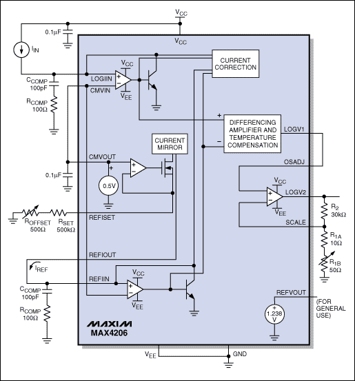
Figure 3. A typical DC log amp, such as the MAX4206, integrates components such as trimmer potentiometers and output amplifiers. Therefore, only a few external components are needed to work properly.
Unlike previous amplifiers, the current logarithmic amplifier integrates all electronic circuits in a tiny package (MAX4206 uses a 4mm x 4mm, 16-pin TQFN package). Prior to 2001, only large DC log amplifiers in DIP packages were available, with 14 to 24 pins. The price of these early products remained between $ 20 and $ 100, while the prices of alternative products are now between $ 5 and $ 15.
Single-supply operation is a new innovation of some modern DC logarithmic amplifiers, which is very suitable for single-supply operation of ADC / system. The MAX4206 can be powered from a single + 2.7V to + 11V power supply or dual power supplies from ± 2.7 to ± 5.5V. The use of a single power supply has the consequence that these logarithmic amplifiers usually maintain a common mode voltage of 0.5V at their input terminals to find the logarithmic BJT with the correct bias. Since these logarithmic amplifiers are current input devices, for most current measurement applications, this internally generated common-mode voltage usually does not cause problems.
Most DC logarithmic amplifiers now generally provide an on-chip current reference. This reference can be connected to the reference input of the logarithmic amplifier, so that the main current input of the logarithmic amplifier can be measured absolutely, rather than proportionally. For the MAX4206, the reference current is generated by a 0.5V DC voltage source, voltage-to-current converter, and a 10: 1 current mirror. An external resistor is required to set the required reference current.
DC logarithmic amplifiers have another new feature. Some logarithmic amplifiers provide an on-chip voltage reference for adjusting the amplifier offset of a general-purpose operational amplifier. The benchmark can also be used for other general purposes.
There is no doubt that most applications of DC logarithmic amplifiers involve optical signal measurement. Two schemes are usually used. In the first scheme, a single photodiode is connected to the logarithmic input, and the reference current is connected to the reference input. The second solution uses two photodiodes, one connected to the logarithmic input and the other to the reference input. When the absolute value of the optical signal strength needs to be measured, the first scheme is adopted, and the second scheme is used for the measurement of the logarithmic ratio of the optical signal strength ("logarithmic ratio").
Figure 4 shows the common circuits of these two schemes. In Fig. 4 (a), a single photodiode measures the optical signal intensity of the optical fiber channel by detecting the optical signal radiated from the optical fiber connector (1%). The picture shows a PIN photodiode. Avalanche photodiodes can also be used to achieve higher measurement sensitivity (if high voltages are used to bias the photodiodes, correct power supply safety measures should be taken). Because the output current of the photodiode is usually linear with the input optical power (the typical value of the photodiode sensitivity is 0.1A / mW), and the MAX4206 can work in five 10-fold dynamic ranges, this circuit can reliably measure 10µW to 1W Optical fiber signal strength. Note that although the MAX4206 can guarantee operation in the temperature range of -40 ° C to + 85 ° C, changes in operating temperature and optical signal frequency can significantly affect the performance of the photodiode. 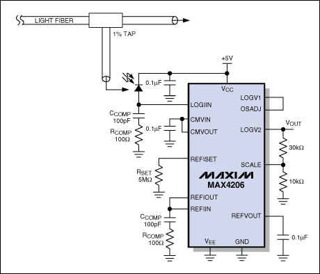
Figure 4a. By placing a photodiode at the input of the logarithmic amplifier, the logarithmic application of measuring the optical signal strength can be easily achieved.
For the case where the photodiode anode is reserved for other circuits, such as the high-speed transimpedance amplifier (TIA) in many fiber optic modules, a precision current mirror / monitor can be placed on the photodiode cathode. MAX4007 series products are very suitable for this application. Please refer to the data sheet of MAX4206 and MAX4007 for more detailed information.
When two photodiodes are used in logarithmic applications, the purpose is to compare the reference light source signal with the reference light signal after attenuation. In this way, the attenuation caused by a given medium can be measured independently of the light signal intensity of the light source (or at least when the light signal intensity does not change much). This application is very common in many optical gas sensors. In Figure 4 (b), the output of the light source is divided equally into two paths. The first path is incident on the reference PIN photodiode, the anode of which feeds into the REFIIN input of the MAX4206. The other path passes through 90 ° specular reflection, passes through the test medium, and enters another PIN photodiode (connected to the LOGIIN input). When the reference photodiode current is calibrated to 1mA, the current of the other photodiode will be less than or equal to 1mA, depending on the attenuation of the optical signal. By locking the reference input current to 1mA or a small value, you can take full advantage of the MAX4206's five 10-fold wide dynamic range. 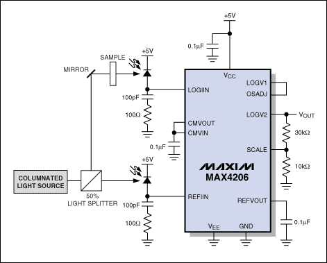
Figure 4b. Log-ratio applications use two photodiodes, which are commonly used to measure optical signal attenuation.
It is worth mentioning that although the MAX4206 does not guarantee operation outside the 10nA to 1mA input current range, the device can usually work beyond this range and still maintain the monotonic relationship between input and output.
Today's DC log amps are still subject to the same restrictions as earlier products. Equation 6 is an ideal approximation of a DC logarithmic amplifier. To get the most accurate expression possible, you must also consider error terms such as gain, bias current, offset, and linearity error. Especially when temperature and time drift cause these errors to be more serious, these aspects need to be considered.
The following equation can more fully reflect the characteristics of BJT-based DC log amplifier: 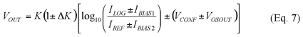
Among them, ΔK is the gain change; IBIAS1 and IBIAS2 are the LOGIIN and REFIIN input bias currents, respectively. VCONF is the log consistency error, and VOSOUT is the output offset. K, ILOG, IREF and VOUT have been defined earlier. In many applications, the error of the bias current is very small relative to the input and reference currents and can usually be ignored in the error expression. The log consistency error is defined as the maximum deviation of the actual output from the ideal logarithmic relationship of Equation 6 (assuming all other error sources have been zeroed). This error usually appears in the form of a difference, so it is easy to check the slight deviation from the ideal curve (Figure 5a). 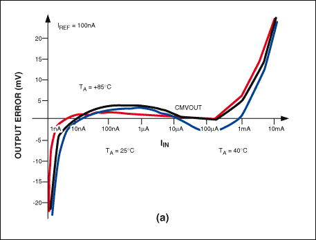
Figure 5a. The logarithmic consistency error curve is usually expressed as a function of input current and operating temperature.
Although its impact will not be immediately reflected, the reference current IREF is the potential largest source of error, which is composed of the initial error, temperature drift and drift caused by device aging. These errors should be considered when evaluating the total error budget of the log amp.
The conversion curve in Figure 5b shows the impact of these actual changes (for demonstration purposes, these effects are exaggerated). The solid black line represents the ideal / expected situation, with a logarithmic intercept of 100nA and a gain of 1V / 10 octave. As indicated by the blue dotted line, the output offset error shifts the solid black line upward or downward. The gain error deflects the offset conversion characteristic curve caused by the offset and is marked by the black dotted line. The blue dotted line reflects the overall effect of nonlinearity and output tolerance error. 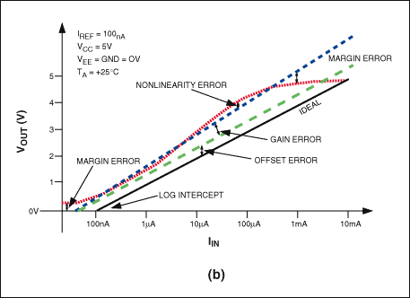
Figure 5b. The effect of different errors given by Equation 7 on the logarithmic transfer function. For clarity, the errors are exaggerated.
In fact, logarithmic amplifier manufacturers have minimized the various errors listed in this section. Using additional calibration and temperature monitoring methods, designers can further reduce the impact of these errors. Designers usually use a calibration table to calibrate after the log amplifier output is digitized.
The performance of the DC logarithmic amplifier is related to the circuit in which it is located. Good design and layout can minimize the impact of input leakage current and the temperature characteristics of the component. However, only good design and layout are usually not enough to ensure the performance required for most logarithmic amplifier applications, especially in the case of large changes in input current and temperature. According to different application requirements and working conditions, appropriate calibration methods should be used to reduce the cumulative error.
When constructing a DC logarithmic amplifier, the following suggestions are available for reference.
Single point calibration This "lowest performance" technique can effectively move the original performance curve (blue dotted line) in Figure 5b up and down so that it can intersect the ideal performance curve (solid black line) at a single point. At a typical operating temperature, the nominal input current and reference current are input to the two inputs of the logarithmic amplifier, respectively, and there will be a deviation between the output and the ideal output. During normal operation, the deviation value is subtracted from the logarithmic amplifier output.
Advantages: The calibration process is rapid, can be performed during the final product testing phase, and does not require a lot of calculations. You can also use a trimming resistor for analog calibration.
Disadvantages: Gain and offset error calibration are performed in a unified manner. When the input and temperature conditions are different from the calibration conditions, the calibration value is invalid.
Two-point calibration is slightly more complicated than the previous calibration technique and can produce better results. It can effectively rotate and move the blue dotted line in Figure 5b up and down to approximate the ideal black solid line. Similarly, the typical operating temperature should be selected. The input current should cross the required working range. If the same reference current is used in both calibration and work, the calibration process can be greatly simplified.
Advantages: The calibration process is relatively fast, which greatly reduces the gain and offset error. Through the gain and offset calculations, digital calibration can be performed; the gain and offset fine-tuning resistors can also be used for analog calibration.
Disadvantages: After input and temperature change, the calibration value is invalid.
Multi-point calibration This technique generates a calibration data table from multiple key sampling points. Sampling is performed at a constant operating temperature. The calibration function is realized by interpolating between sampling points.
Advantages: Since you can select a large number of important input conditions, you can greatly reduce gain, offset, and nonlinear errors.
Disadvantages: Some form of interpolation is required, which increases the amount of calculation. After input and temperature changes, the calibration fails.
Temperature adjustment calibration is similar to multi-point calibration. This technology also considers the test temperature and adds an additional independent variable.
Advantages: This technique greatly reduces the effects of gain, offset, non-linear errors, and temperature changes on the total error. It is a good choice for high-performance, small batch products.
Disadvantages: Because the calibration is performed across the entire temperature range, the calibration time of the final product testing phase is greatly extended. The multi-dimensional interpolation operation of sampled data requires more computing resources. An additional temperature monitoring circuit is also required.
Maintain proper input tolerance. The output of the log amp should not be close to the power supply swing. This is because when it is close to the power swing, its ability to source and sink current is limited. When the current you are trying to measure is close to or lower than the reference current, or close to the maximum input current, it is easy to ignore this recommendation. The selected reference current should be lower than the minimum input current. Carefully set the gain to ensure that at the maximum input current, the output will not reach the maximum output voltage of the logarithmic amplifier. Dual-supply logarithmic amplifiers will also help solve this problem, because in most designs, the same input and reference current keep the amplifier output at an intermediate value.
Advantages: improved accuracy and response time under extreme input conditions.
Disadvantages: The available output range is slightly reduced.
Component selection uses the same type of external resistor with a low temperature coefficient. This is especially important for resistors whose resistance value affects performance (for example, reference current generating circuits). For parameters affected by the resistance ratio, such as gain and offset, the effect of temperature changes is small. The temperature stability of the compensation element is generally not critical. In order to avoid leakage problems when measuring small currents, low leakage PCB materials should be considered.
Advantages: Minimize performance degradation caused by external components.
Disadvantages: Low temperature coefficient components are generally slightly more expensive, but considering they can significantly improve performance, it is still worth the money.
Keep the temperature environment consistent. No part of the log amp circuit should be at a significantly different temperature than the rest of the circuit. This precaution can ensure that temperature changes have the same effect on all circuits as much as possible.
Advantages: Extra independent variables are eliminated during calibration.
Disadvantages: May cause inconvenience to layout and overall circuit design.
In short, DC logarithmic amplifiers have been developed into small, easy-to-use, cost-effective circuits that are very suitable for certain analog designs. The logarithmic function can easily compress signals with a wide dynamic range and linearize the exponential sensor. Digitizing a wide dynamic range signal requires a high-resolution ADC, and the compression function of the logarithmic function supports the use of a low-resolution ADC. The circuit implementation of the DC logarithmic amplifier IC is relatively intuitive, and performance optimization can be achieved with very little effort. Calibration can improve the performance of logarithmic amplifiers, but not all applications must be calibrated.
We are the leading and innovative manufacturer with professional research and development capacity in China.Now the product cover Micro USB to USB,
micro USB Connector,Micro USB 2.0 Cable. Etc.
Product information
This Micro Usb data cable can be connected to all the smart devices with MICRO interface to your computer USB port for sync and charging .
Data cable for synchronizing and recharging your phone
USB 2.0-compatible port
Data synchronization
Charges phone from your computer
Charges phone from a USB charger
Compatible with phones with a MICRO USB connector
Micro USB Cable, Micro USB to USB, USB Connector, Micro USB 2.0 Cable
Hebei Baisiwei Import&Export Trade Co., LTD. , https://www.baisiweicable.com