Abstract: This applicaTIon note discusses how to connect various Dallas Semiconductor T1 / E1 / J1 single-chip transceivers (SCTs) or line interface units (LIUs) for 1 + 1 redundancy. It contains a simple hardware design without relays and software register setTIngs for specific devices. A designer can use these drawings to implement an operaTIonal system quickly.
OverviewHitless protecTIon describes the ability to switch between the primary and backup line card without losing framing synchronization when a primary line-card failure occurs. This feature ensures that telecommunications equipment will provide uninterrupted or continuous service and maintain an extremely high-reliability rating.
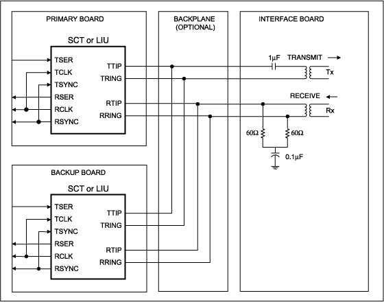
Figure 1. An example of typical connections for a system that provides hitless protection and eliminates the need for bulky mechanical relays.
One-to-one (1 + 1) redundancy refers to a configuration where each line card has a dedicated backup card waiting in case of failure. N + 1 redundancy describes a configuration in which multiple cards have only one backup card to share among them . These traditional protection designs often required the use of relay modules to switch the signal between the primary and the backup line card.
There are three notable disadvantages to using relays. Firstly, relay switching times are slow, which causes data corruption on the line. This data corruption results in bit errors, data loss, and perhaps a loss-of-frame condition. A loss-of -frame condition exacerbates the problem because it takes a considerable amount of time to reframe, during which all data is misaligned and, therefore, garbage. Secondly, the relay modules are bulky and occupy valuable board space. Finally, the relay modules require a considerable amount of power when used on boards with multiple T1 / E1 lines.
Figure 1 shows a redundant scheme that supports hitless protection. The backup transceiver is receiving and framing in parallel with the primary transceiver. This is possible because the Dallas Semiconductor line interface units are designed with high-impedance receive inputs and transmitter outputs that can be tri -stated. Therefore, the backup line card inputs and outputs do not affect the signal that the primary line card is transmitting and receiving. This type of configuration eliminates the need for bulky mechanical relays.
Microprocessor-Controlled SwitchingTo switch from the primary LIU card to the backup card, the following steps need to be performed: Disable the transmit current limiter of the primary LIU and the backup LIU. Enable the backup transmitter while the primary transmitter is still operating. Disable the primary transmitter by tri-stating its output drivers. Enable the transmit current limiter of the primary LIU and the backup LIU. Tables 1, 2, 3, and 4 list the register bits that need to be set or cleared.
Table 1. Register Settings for the DS2155 Single-Chip Transceiver
Table 2. Register Settings for the DS21352 and DS21552 Single-Chip Transceivers
Note: The TEST2 register may also be referred to as LITEST2 in some DS21352 / DS21552 documentation.
Table 3. Register Settings for the DS21354, and DS21554 Single-Chip Transceivers
Note: The TEST3 register may also be referred to as LITEST2 in some DS21354 / DS21554 documentation.
Table 4. Register Settings for the DS21 (Q) 348 and DS21 (Q) 48 Line Interface Units
Receive-Side Software-Selected TerminationThe DS2155, DS21 (Q) 348, and DS21 (Q) 48 devices have internal software termination available, so steps must be taken to ensure that the receive-side line interface is configured properly. When two pairs of receiver inputs are connected to the transformer, only one device can control the software-selected termination. Having software-selected termination enabled on both devices would result in a line impedance mismatch and improperly terminated signals. To ensure that these problems do not occur, simply have software-selected termination enabled only on the active line card (the line card currently recovering the signal) and disabled on the other. When the active card is removed or swapped from the system, simply switch whichever card is currently performing the software termination function . Information on enabling and disabling the internal software termination can be found in the product data sheet. Power-up and Hot-SwappingThese SCT and LIU de vices have other features that must be considered when powering-up the system and replacing a bad line card. Upon power-up, the DS2155 will clear its registers space, which leaves the device's transmit drivers tri-stated. Tri-state is the ideal condition for the redundancy application because it prevents a card from interfering with another card that is already transmitting data.
Older generation devices (ie, the DS21352, DS21552, DS21354, DS21554, DS21 (Q) 348, and DS21 (Q) 48) will power-up with the transmitter drivers turned on. To prevent this condition from occurring, the user must implement the following in the system: Wire the TEST pin so that the default state is a high. This will tri-state all output and I / O pins, the parallel control port, and the transmitter outputs. In this state, the processor will be able to perform write operations to the parallel port, but read operations will not work. Initialize the device by writing 0x00 to the entire register addresses range. Disable the transmitter of the device using the register bits mentioned in Tables 1, 2, 3, and 4. Set the TEST pin state low to enable regular device operation. Test Results A test and simulation setup was designed to ensure that the DS2155 devices will operate in a hitless-protection switching system. The test setup is presented below. The four scope plots presented in Figures 2 through 5 demonstrate that the transmit pulse template is met when the two devices are coupled together in a hitless-protection switching system. The pulse templates are divided into T1 and E1 pulses, and each has a scope plot for both port 1 and port 2.
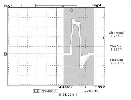
Figure 2. T1 pulse shape for port 1.
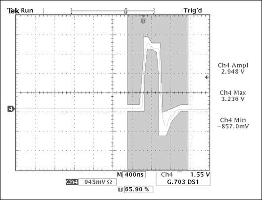
Figure 3. T1 pulse shape for port 2.

Figure 4. E1 pulse shape port 1.
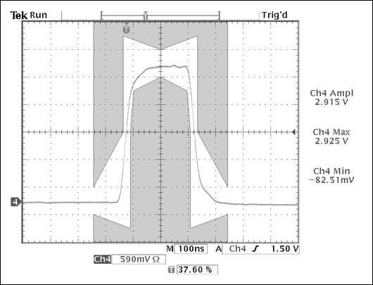
Figure 5. E1 pulse shape port 2.
Test SetupThe test setup in Figure 6 was used to generate the pulse template scope shots in Figures 2 though 5. The setup consisted of a modified DS21Q55 demonstration kit, an Acterna T1 Fireberd, an Acterna E1 Fireberd, and a Tektronix® TDS 3054 with pulse mask option and differential signal adapter. The DS21Q55 was used instead of two DS2155 devices because the DS21Q55 board was readily available and switching between the primary and backup device could be done in software using the DS21Q55 demonstration kit. Since the DS21Q55 is actually four DS2155 devices placed on a single board, the DS21Q55 results should not differ from those that would be obtained using two DS2155 devices. The board was modified so that the DS21Q55's ports 1 and 2 shared the same network interface circuit on the two transmit ports and two receive ports . To simulate the longer than normal tip and ring-signal routes that would be present in a real-world system, 60 inches of twisted pair cable were used between the transformer and the tip and ring signals on the DS21Q55. The extra distance did not degrade the performance of the DS21Q55 transmitter or receiver in any way.
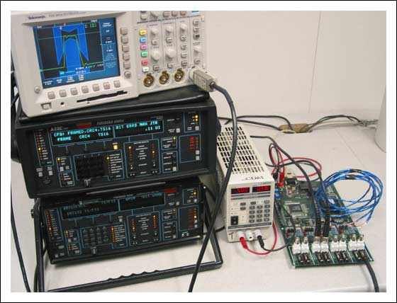
Figure 6. Hitless-protection switching test setup.
OverviewHitless protecTIon describes the ability to switch between the primary and backup line card without losing framing synchronization when a primary line-card failure occurs. This feature ensures that telecommunications equipment will provide uninterrupted or continuous service and maintain an extremely high-reliability rating.
Figure 1. An example of typical connections for a system that provides hitless protection and eliminates the need for bulky mechanical relays.
One-to-one (1 + 1) redundancy refers to a configuration where each line card has a dedicated backup card waiting in case of failure. N + 1 redundancy describes a configuration in which multiple cards have only one backup card to share among them . These traditional protection designs often required the use of relay modules to switch the signal between the primary and the backup line card.
There are three notable disadvantages to using relays. Firstly, relay switching times are slow, which causes data corruption on the line. This data corruption results in bit errors, data loss, and perhaps a loss-of-frame condition. A loss-of -frame condition exacerbates the problem because it takes a considerable amount of time to reframe, during which all data is misaligned and, therefore, garbage. Secondly, the relay modules are bulky and occupy valuable board space. Finally, the relay modules require a considerable amount of power when used on boards with multiple T1 / E1 lines.
Figure 1 shows a redundant scheme that supports hitless protection. The backup transceiver is receiving and framing in parallel with the primary transceiver. This is possible because the Dallas Semiconductor line interface units are designed with high-impedance receive inputs and transmitter outputs that can be tri -stated. Therefore, the backup line card inputs and outputs do not affect the signal that the primary line card is transmitting and receiving. This type of configuration eliminates the need for bulky mechanical relays.
Microprocessor-Controlled SwitchingTo switch from the primary LIU card to the backup card, the following steps need to be performed: Disable the transmit current limiter of the primary LIU and the backup LIU. Enable the backup transmitter while the primary transmitter is still operating. Disable the primary transmitter by tri-stating its output drivers. Enable the transmit current limiter of the primary LIU and the backup LIU. Tables 1, 2, 3, and 4 list the register bits that need to be set or cleared.
Table 1. Register Settings for the DS2155 Single-Chip Transceiver
| Step | Action | DS2155 Register Address |
| 1 | Set Primary and Backup LIC2.1 = 1 | 0 x 79 |
| 2 | Set Backup LIC1.0 = 1 | 0 x 78 |
| 3 | Set Primary LIC1.0 = 0 | 0 x 78 |
| 4 | Set Primary and Backup LIC2.1 = 0 | 0 x 79 |
Table 2. Register Settings for the DS21352 and DS21552 Single-Chip Transceivers
| Step | Action | DS21352 / DS21552 Register Address |
| 1 | Set Primary and Backup TEST2.4 = 1 | 0 x 09 |
| 2 | Set Backup LICR.0 = 0 | 0 x 7C |
| 3 | Set Primary LICR.0 = 1 | 0 x 7C |
| 4 | Set Primary and Backup TEST2.4 = 0 | 0 x 09 |
Note: The TEST2 register may also be referred to as LITEST2 in some DS21352 / DS21552 documentation.
Table 3. Register Settings for the DS21354, and DS21554 Single-Chip Transceivers
| Step | Action | DS21354 / DS21554 Register Address |
| 1 | Set Primary and Backup TEST3.4 = 1 | 0 x AC |
| 2 | Set Backup LICR.0 = 0 | 0 x 18 |
| 3 | Set Primary LICR.0 = 1 | 0 x 18 |
| 4 | Set Primary and Backup LITEST2.4 = 0 | 0 x AC |
Note: The TEST3 register may also be referred to as LITEST2 in some DS21354 / DS21554 documentation.
Table 4. Register Settings for the DS21 (Q) 348 and DS21 (Q) 48 Line Interface Units
| Step | Action | DS21348 / DS2148 Register Address |
| 1 | Set Primary and Backup CCR2.5 = 1 | 0 x 01 |
| 2 | Set Backup CCR4.0 = 0 | 0 x 03 |
| 3 | Set Primary CCR4.0 = 1 | 0 x 03 |
| 4 | Set Primary and Backup CCR2.5 = 0 | 0 x 01 |
Older generation devices (ie, the DS21352, DS21552, DS21354, DS21554, DS21 (Q) 348, and DS21 (Q) 48) will power-up with the transmitter drivers turned on. To prevent this condition from occurring, the user must implement the following in the system: Wire the TEST pin so that the default state is a high. This will tri-state all output and I / O pins, the parallel control port, and the transmitter outputs. In this state, the processor will be able to perform write operations to the parallel port, but read operations will not work. Initialize the device by writing 0x00 to the entire register addresses range. Disable the transmitter of the device using the register bits mentioned in Tables 1, 2, 3, and 4. Set the TEST pin state low to enable regular device operation. Test Results A test and simulation setup was designed to ensure that the DS2155 devices will operate in a hitless-protection switching system. The test setup is presented below. The four scope plots presented in Figures 2 through 5 demonstrate that the transmit pulse template is met when the two devices are coupled together in a hitless-protection switching system. The pulse templates are divided into T1 and E1 pulses, and each has a scope plot for both port 1 and port 2.
Figure 2. T1 pulse shape for port 1.
Figure 3. T1 pulse shape for port 2.
Figure 4. E1 pulse shape port 1.
Figure 5. E1 pulse shape port 2.
Test SetupThe test setup in Figure 6 was used to generate the pulse template scope shots in Figures 2 though 5. The setup consisted of a modified DS21Q55 demonstration kit, an Acterna T1 Fireberd, an Acterna E1 Fireberd, and a Tektronix® TDS 3054 with pulse mask option and differential signal adapter. The DS21Q55 was used instead of two DS2155 devices because the DS21Q55 board was readily available and switching between the primary and backup device could be done in software using the DS21Q55 demonstration kit. Since the DS21Q55 is actually four DS2155 devices placed on a single board, the DS21Q55 results should not differ from those that would be obtained using two DS2155 devices. The board was modified so that the DS21Q55's ports 1 and 2 shared the same network interface circuit on the two transmit ports and two receive ports . To simulate the longer than normal tip and ring-signal routes that would be present in a real-world system, 60 inches of twisted pair cable were used between the transformer and the tip and ring signals on the DS21Q55. The extra distance did not degrade the performance of the DS21Q55 transmitter or receiver in any way.
Figure 6. Hitless-protection switching test setup.
Tektronix is ​​a registered trademark of Tektronix, Inc.
Rainproof Cummins Diesel Generator
Waterproof Diesel Generator,Rainproof Cummins Diesel Generator,600Kw Cummins Rainproof Generator,600Kw Rainproof Cummins Diesel Generator
Jiangsu Lingyu Generator CO.,LTD , https://www.lygenset.com