Handheld product designers such as cell phones, digital cameras, MP3 players and personal digital assistants (PDAs) continue to face the challenge of providing more features in a smaller form factor. Integrated circuit (IC) designers are driving this trend by increasing the speed and performance of devices while reducing the size of silicon devices, enabling space-constrained portable electronics to use the high-speed data line interfaces required to support added functionality. But what is the cost? In order to achieve higher functionality in a smaller area for portable applications, IC technology uses smaller geometries and lower operating voltages, making them more susceptible to electrostatic discharge (ESD) voltage damage. sensitive. This trend has a negative impact on the reliability of the end product and increases the likelihood of field failures. At the same time, portable device designers have to find an off-chip ESD protection solution that combines low capacitance and low ESD clamping voltages, and is packaged small enough to accommodate today's shrinking portable electronic applications.
This article refers to the address: http://
Consideration of choosing an effective ESD solution
There are three main considerations for choosing an effective portable electronic product for high-speed ESD solutions: size, capacitance, and ESD clamping capability. Package size requirements are determined by the designer, but a general guideline for portable products is "the smaller the better."
For high speed data lines, adding capacitance can reduce signal integrity. Capacitors can increase the data line by designing components and the board itself. When designers begin to add ESD protection, there is very little space left to add extra capacitance. Each design is different and the requirements for ESD protection capacitors may vary, depending on the total capacitance budget used by other design components, but a general rule is that the lower the capacitance, the better.
This article will focus on the most popular high-speed interface for portable applications, namely USB 2.0 (480 Mb/s). At this data rate, the protection solution must have a capacitance of less than 1.5pF to maintain data line integrity.
The ultimate consideration in choosing an effective ESD solution is the ESD clamping capability. The purpose of the ESD protection device is to reduce thousands of ESD input voltages to the IC's protected safe voltage and shunt current to the IC. Although the input voltage and current of the required ESD waveform have not changed over the past few years, the level of safe voltage required to protect the IC is reduced. In the past, IC design was more robust to ESD and could handle higher voltages, so it is sufficient to choose any protection diode that can survive IEC61000-4-2 level 4. In the face of newer, more sensitive ICs, designers now need to ensure that protection devices can survive the IEC61000-4-2 level 4 standard, and that the protection device will clamp the ESD pulses at a low enough voltage to This ensures that the IC is not damaged. When choosing the best protection device for a given application, the designer must consider how the ESD protection device clamps the invading ESD. IC sensitivity varies from design to design, but a general guideline for clamping voltage is "the lower the clamping voltage, the better."
When selecting an ESD protection component, the package size and capacitance can be easily determined by looking at the product data sheet. However, it is a bit cumbersome to define the clamp voltage because there is no relevant standard that specifies how to measure the clamp voltage in an ESD event. This article will focus on how to detect the clamping voltage of an ESD protection diode.
ESD waveform
The most common waveform that defines a typical ESD event at the system level is the IEC61000-4-2 waveform, which is distinguished by its sub-nanosecond rise time and high current level. The specification of this waveform involves four levels of ESD pulse amplitude. Most designers need to make the product meet the highest level of 8kV contact discharge or 15kV air discharge requirements.
The data sheet for most ESD protection components will be marked with the maximum rated voltage in accordance with IEC61000-4-2, which indicates that the component will not be damaged by the specified level of ESD pulses. However, this rated voltage does not give any clamp voltage information about high frequency, high current transient events such as ESD. The clamping voltage of the protection diode is much higher when these transient events occur compared to the DC (DC) breakdown voltage specified on the data sheet. However, it is difficult to specify the clamp voltage of the IEC61000-4-2 specification because it is intended to be a system-level pass/fail specification. In order to apply this specification to the protection component, it is important not only to check whether the protection component passes or not, but also how it clamps the ESD voltage to the low level and how it performs in protecting the sensitive component.
The best way to compare the protection diode clamping voltage is to use an oscilloscope to take a screenshot of the actual voltage waveform across the diode during an ESD event. This can be achieved by the test setup shown in Figure 1.
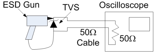
Capture test settings for ESD clamp voltage screenshots
This test setup will give the voltage waveform through the protection element when an ESD event occurs, which will show the voltage level that the IC along this line will experience during the ESD event. When looking at the voltage waveform of the ESD protection device in the IEC61000-4-2 test, it can be seen that there is usually an initial voltage spike followed by a second spike, and the final voltage waveform will tend to level. The initial voltage spike is caused by the overshoot of the initial current spike and test structure in the IEC61000-4-2 waveform. However, the initial spike duration is shorter, which limits the amount of energy delivered to the IC. The clamping performance of the protection device is best seen in the curve after the initial overshoot. The second spike is the main problem, because the voltage waveform at this time lasts longer, increasing the total energy that the IC will suffer. In the following study the clamp voltage is defined as the maximum voltage of the second spike.
High-speed data line protection options
There are two main ESD protection options, the right size and capacitance specifications for USB2.0 high speed protection for portable applications, passive and silicon devices. In the benchmark study below we will look at the key specifications for these two types of products under common examples. For a fair comparison, the various techniques in the options we will use are all in the same package size.
Passive protection device
Technology: Tyco/Raychem polymer based varistor single line protection
Package size: 1.0 × 0.5mm (also known as 0402)
Capacitance specified on the data sheet: 0.25pF
Technology: Innochips "ESD Suppressor" Single Line Protection
Package size: 1.0 × 0.5mm (also known as 0402)
Capacitance: 0.15pF
Silicon protection device
Technology: Semtech Railclamp single line protection
Package size: 1.0 × 0.6mm (also known as 0402)
Capacitance: 0.3pF
Technology: ON Semiconductor's "Integrated ESD Protection" Single Line Protection
Package size: 1.0 × 0.6mm (also known as 0402)
Capacitance: 0.5pF
analysis
All of these options are tested using the popular ultra-small 0402 size package, which is small enough to fit most portable designs. They also have capacitances well below the 1.5pF requirement. For the USB 2.0 high-speed version of 480Mb / s data rate, any capacitance below 1pF will be able to maintain the signal integrity of the data line, any difference is difficult to detect. The key performance difference between these products lies in the ESD clamping performance. Passive components have the highest clamping voltage during an ESD event, reaching 67V to over 70V. The clamping voltage of the Semtech silicon protection device is 45V for positive pulses and 44V for negative pulses. ON Semiconductor's silicon protection devices clamp the ESD event to 15V during positive ESD pulses and to 10V during negative ESD pulses.
Silicon devices with lower clamping voltages perform better than passive components. However, what's interesting is that the same silicon protection devices, Semtech's Railclam technology and ON Semiconductor's "integrated ESD protection" technology also have important differences. The design techniques used to implement each type of technology are able to determine how they clamped to the ESD pulse. Many design techniques for reducing capacitance are accompanied by a compromise with higher ESD clamping voltages. To overcome this design tradeoff without sacrificing clamp voltage performance, ON Semiconductor uses groundbreaking process technology to integrate ultra-low capacitance pin diodes and high-power transient voltage suppressor (TVS) diodes onto a single die. A high performance off-chip ESD protection solution. This new integrated ESD protection technology platform maintains the excellent clamping and low leakage performance of traditional TVS diode technology while reducing the capacitance to 0.5pF. This leads the industry in clamping performance to ensure the protection of the most sensitive integrated circuits.
Radio Fence,E-Dog Fence,Wireless Invisible Fence,Above Ground Electric Dog Fence
Elite-tek Electronics Ltd , https://www.aetertek.ca