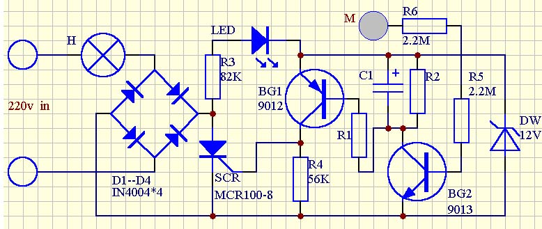
| Circuit principle: The delay switch circuit is shown in Figure D1-D1. SCR constitutes the main circuit of the switch, and BG1, BG2 etc. constitute the control circuit of the switch.
Normally, both BG1 and BG2 are in the cut-off state, the SCR is blocked, and the electric lamp H is off. At this time, 220V AC is rectified by D1--D4, R3 and DW make the LED glow, which is used as the night switch position. At this time, the current flowing through H is only about 2 mA, which is insufficient to make the lamp H emit light. When it is necessary to turn on the light, only touch the electrode sheet M with your finger, and the leakage current of the human body is injected into the base of BG2 through R5 and R6, and BG2 is quickly turned on. The collector of BG2 is at a low level, and BG1 is turned on accordingly. Therefore, a trigger current is injected into the SCR control electrode through BG1 to turn on the SCR, and the lamp H is turned on to emit light. At the instant of BG2 conduction, C1 is connected in parallel with the two ends of DW through the ce pole of BG2, so it is quickly charged with a voltage of about 12V. After the lamp is lit, the human hand leaves M. Although BG2 returns to the off state, the charge stored in C1 is discharged to the BG1 via R1 to discharge the junction, so that BG1 remains on, so the lamp continues to shine. When the charge of C1 is basically discharged, BG1 returns to the cut-off state, and the SCR loses the trigger current. When the AC power crosses zero, the SCR is turned off and the lamp goes out.
The switching delay time is mainly determined by the values ​​of resistors R1, R2 and capacitor C1. The following provides a set of experimental data for your reference. If you want to further increase the delay time, you can increase the capacity of C1. In addition to the above main factors, the magnification of BG1 and the trigger sensitivity of SCR also have an effect on the delay time. |