Frequency selective amplifier |
| 1. Working principle and frequency characteristics of double T bridge |
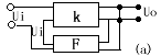
| Frequency-selection amplifier, which selects a desired frequency signal from a variety of frequency input signals and amplifies the block diagram shown in the figure below can form a frequency-selection amplifier circuit, where block K is the basic amplifier circuit and block F is Frequency selection negative feedback network, therefore, frequency selection amplifier is essentially a negative feedback circuit with frequency selection. The closed-loop benefit of the circuit is KF = K / (1 + FK) Where: K = U O / U i is the open loop gain F = U F / U O is the feedback coefficient |
 | 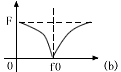 |  |
| Generally, the RC frequency selection network is used to realize the selection period. Figure (b) shows the variation curve (frequency characteristic) of the feedback coefficient F with the frequency f. When f = fo, then F = 0. Therefore, for the resonance frequency fo, the amplifier circuit does not have negative feedback, so K F = K, at this time the output voltage of the amplifier is the largest. As the frequency moves away from fo, F increases rapidly, and the corresponding KF also quickly decay to zero. See figure C. Therefore, the output voltage of other useless frequencies that deviate from the fo point is also very small, as for the attenuation of KF The speed is mainly determined by the frequency selection characteristics of the feedback network. The RC frequency selection network with double T bridge is usually used. In actual use, there are two most commonly used: |
 |
| The other is an asymmetric double T bridge as shown in the figure above. Assuming that the internal resistance of the power supply RS = 0 and the load RL = 00, the calculation formula is as follows: Resonance angular frequency ω O = 1 / RC --------------------- 1 type quality factor Q = [1/2 (1 + a)] = [fo / 2 △ fo .7 ] --------- 2 The modulus and amplitude angle of the transmission coefficient (feedback coefficient) are: |
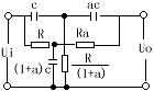
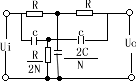
φ = arctg1 / QY In the formula: Y = σ- (1 / σ) is the generalized detuning coefficient σ = f / fo is the relative detuning coefficient ----------------------- Type 4 2 △ fo.7 The bandwidth of the main half-power point can be seen from the formula 2: For a fixed resonance frequency fo, the larger the Q, the narrower the passband; conversely, the smaller the Q, the wider the passband, therefore, Q The size can reflect the selectivity of the double T network. The advantage of this double-T bridge is that Q is large, but the input impedance is low, the output impedance is high, and it is inconvenient to connect with the amplifier. Due to the different parameters of the bridge arm, the selection and adjustment also cause trouble. Asymmetrical double T circuit, the input, output impedance and phase angle change of this circuit, please refer to the top chart, where a is usually selected (0.1-0.2) to get a larger Q value. The second type is a symmetrical double T circuit, as shown in Figure 3 below, and the calculation formula is as follows: | |
| Resonance frequency: ω0 = | |
| Quality factor: Q = |
| Obviously, Q is related to n, when n = 1, then Qmax = 0.25, but the adjustment is inconvenient. For the convenience of adjustment, n = 0.5 is often selected, corresponding to the value of three resistors is equal; or n = 2, corresponding to three The capacitance values ​​are equal. Due to the symmetrical double T bridge, it is more convenient to select components and adjust, so it is widely used. Correction method for asymmetry of transmission characteristics: Actual use, because R S ≠O and R L ≠OO and sometimes double-T network and the amplifier AC coupling of Fig 4 (A), a signal source (E S and R S) C S with a double T coupled via , When the frequency is zero, the capacitive reactance 1 / ω C S is infinitely large, so F = O; and when the frequency is high, the capacitive reactance of C S , C 2 , and C 3 is very small, at this time F is approximately RL / (R L + R S ); Since Z S and R L do not affect the resonance frequency, when f = fo, F = 0; therefore, the curve of F with frequency changes is shown in Figure 4 (B), which can be seen from the figure , The transmission characteristics are asymmetric |
 |
| Z 3 and L is present in R F is not only makes the amplitude-frequency characteristic distortion, but it also generates an asymmetric phase-frequency characteristics, if the mobile phase in the vicinity of the resonance point than π / 2, plus an additional phase shift of this action In this closed-loop amplifier circuit, positive feedback is introduced and self-oscillation occurs. In order to eliminate this undesirable phenomenon, the capacitor C L is connected in parallel at the both ends of R L in the circuit diagram 4 (A), and the amplitude and phase characteristics of F can be corrected under the action of C L as shown in FIG. 4 (B). , Should satisfy the following relationship: R 1 C 1 = R 2 C 2 = R L C L = R S C S R1R2 = (1 + n) RLRS If the coupling capacitor is connected to the load terminal, the capacitor C S must be connected in parallel at the input terminals 1 and 1 '. The ideal correction condition is still the same as the above relationship. If the direct coupling method is used for double T and amplifier, it is not necessary to connect C S or C L , at this time, the symmetry conditions of the amplitude and phase shift characteristics of F can be simplified as: R 1 R 2 = (1 + n) R S R L R 1 C 1 = R 2 C 2 It must be noted that: (1) The double T network is directly coupled with the amplifier. Although the selectivity is high, the DC operating point will be affected, and adjustment is difficult; (2) The internal resistance Z S should be reduced as much as possible and the load Z L should be increased as much as possible, otherwise the selectivity of double T will be significantly reduced, so the basic amplifier circuit should be connected to the emitter follower or source follower before and after To meet the requirements of the double T network, (3) Under the influence of the error of the elementary parameter, the balance condition of the double T will also be destroyed, and the amplitude frequency and phase frequency characteristics will change. Therefore, the components of the double T network should be in accordance with the specific The requirements must be strictly selected components with good temperature characteristics and stable operation, and must be aged |
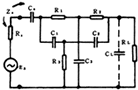 Figure 4 (A) | 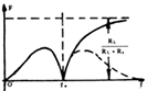 Figure 4 (B) | 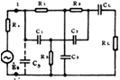 Figure 4 (C) |
| Second, the connection mode of the double T bridge and the amplifier |
| The connection method of double T bridge and amplifier is shown in the table below |
|
| 3. Practical circuit analysis and adjustment method 1. Circuit analysis |
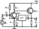
| Figure 5 is a fixed frequency transistor frequency selective amplifier circuit, the resonance frequency is 100 Hz, the passband is less than 6 Hz, the gain of the resonance point | KF | = 70, it belongs to the first type of frequency selective amplifier circuit, composed of BG 1 and BG 2 Common injection amplifier circuit, the input signal U i and the feedback voltage U F are added to the bases of the two tubes [U F is first sent to the base of BG 2 through the beam follower BG 4 ], and its function is: on the one hand, it increases frequency selective amplification The input resistance of the circuit, on the other hand, can increase the load resistance of the double T [that is, the input resistance of the BG 4 ] to eliminate the influence of the internal resistance R S of the input signal source on the double T. BG 3 is also an emitter follower, which makes the double T The internal resistance of the power supply is reduced, thereby improving the selectivity of the circuit. The double T bridge is asymmetrical, it is AC coupled with the amplifier circuit, so CL is used to correct the symmetry of the amplitude-frequency phase-frequency characteristics. |
 Figure 5 |
| 2. Adjustment method |
| In order to reduce the requirements for accuracy and ease of Tiaohulishan resistance section, R 2 (or R 3) respectively, a fixed resistor R '2 (or R' 3) and a potentiometer R '2 (or R' 3) composed of potentiometer The value is 10-20% of R 2 (or R 3 ) is appropriate [if fixed resistance, the error is 5%], and then select the capacitor according to the required accuracy. |
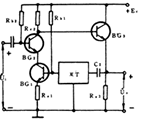
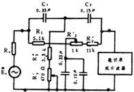 Image 6 |
| Adjustment steps (1) Perform coarse adjustment according to the double T network of the circuit in Figure 6. The signal source is selected at a frequency of 100 Hz and the input voltage is greater than 2 volts. Then repeatedly adjust the potentiometers R'2 and R'3 to minimize the output voltage. For fixed-point frequency For the double T network, it is not difficult to make Fmin = 0.002 (that is, the attenuation is 54 dB). Note that in the circuit of Figure 5, for the double T network, the right side is the input terminal and the left side is the output terminal. In addition, the signal source is not The linear distortion should be small, otherwise it is difficult to make Fmin = 0.002. (2) Adjust the DC operating point of the amplifier, Since the basic amplifying circuit is directly coupled to the amplifier, the operating point to each other at all levels have been implicated, so long as the adjustment of the bias Rb1, R b2 Ue 3 so as to 6-7 volts. (3) Adjust the gain of the amplifier without feedback (open loop), adjust the input amplitude from the BG1 base input signal (f = 100 and Hertz) so that the output waveform is not distorted, and find K = U O / U i = 70, if If K> 70, then Re 2 is decreased; on the contrary, if K <70, Rc 2 can be increased until K = 70. (4) Fine adjustment of the double T bridge into the double T bridge, because the double T has been adjusted to f = 100 Hz and Fmin≈0, and because the input impedance of the double T is much larger than the output impedance of the amplifier, so connect After entering the double T bridge, the negative feedback is zero for the resonance point. Therefore, the gain of the amplifier should not be affected. According to this principle, if the K is slightly less than 70 after being connected to the double T network (because the double T always has a load effect), it means that the circuit is working normally; if the double T network is connected , K is greater than 70, then the introduction of a double T positive feedback at the resonance point, then should transfer large R '3, so that K is reduced to 70; double T and vice versa when the access network, larger K decreases, then the double T at resonance Fmin ≠O, so negative feedback, so that K is reduced, less time may be appropriate adjusted R '3, is increased up to 70 K Wushi. During the debugging process, if self-excited phenomenon is found, the self-excited should be eliminated first, and then debugged. There are three types of self-excited oscillation 1. Self-excited near the resonance point, because the double T bridge near fo produces positive feedback, R 3 can be adjusted to eliminate self-excitation. 2. At very low frequencies (about a few Hertz), it is due to the asymmetry of the amplitude-frequency and phase-frequency characteristics of the double-T network. At very low frequencies, the coupling capacitance or side of the amplifier The circuit capacitor will introduce additional phase shift, which constitutes positive feedback. Therefore, to eliminate such self-excited vibration pin, you can use a direct coupling discharge circuit or reduce the value of the coupling capacitor and bypass capacitor, especially pay attention to the double T network and The effect of the coupling capacitance of the amplifier C4; 3. The elimination method of high-frequency self-oscillation (about tens of kilohertz) is to shrink the passband of the amplifier to attenuate the high-end gain quickly. For example, connect Cm in the circuit of Figure 5 to make BG The load of 2 becomes R 2 in parallel with Cm, and the value of Cm is selected so that at low frequencies, Cm does not work, and near the self-excitation frequency, the impedance of BG 2 is suddenly reduced sharply, thereby making the self-excitation eliminate |
Reverse Conducting Thyristor(RCT) is also called Reverse- appreciation Thyristor.The characteristic is that a diode is connected in reverse parallel between the anode and cathode of thyristor, so that the transmitting junction of anode and cathode is short-circuited.As a result of this special circuit structure, it has high voltage resistance, high temperature resistance, short turn-off time, low switching voltage and other good performance.For example, the turn-off time of the reverse thyristor is only a few microseconds, and the working frequency is dozens of KHZ, which is better than the fast thyristor (FSCR).This device is suitable for switching power supply and UPS uninterrupted power supply. One RCT can replace one thyristor and one continuous current diode respectively.
Reverse Conducting Thyristor(RCT)
Reverse Conducting Thyristor,Original Reverse Conducting Thyristor,New Reverse Conducting Thyristor,Reverse-Conducting Thyristor 2200V
YANGZHOU POSITIONING TECH CO., LTD. , https://www.yzpst.com