As a kind of wireless access communication method, short-range wireless data communication can be widely used in the fields of remote control, alarm, telemetry and the like. Designing RF transceivers using RF transceivers is an important way to achieve near-distance information transmission. This article is based on Infineon's RF transceiver TDA5255 and XC866 microcontroller to design an RF transceiver to achieve information transmission.
2 TDA5255 RF Transceiver2.1 Main features
The TDA5255 is a low power, single-chip FSK/ASK transceiver for half-duplex low data rate communications from 433 MHz to 435 MHz. The device has high integration and simple peripheral circuits. Internally includes power amplifier, low noise amplifier, AGC control circuit, double balanced mixer, synthesized converter, I/Q limiter, RRSI generator, FSK demodulator, fully integrated VCO and PLL synthesizer, Tuned crystal oscillator, data filter, data comparator, positive and negative peak detector, data rate detection circuit and bus interface, also provides low power mode, low current consumption (receive mode 9 mA, transmit mode 12 mA) The power supply voltage is 2.1 V to 5 V, FSK/ASK modulation and demodulation, I2C/3-wire microcontroller interface, internal low-pass channel selection filter and data filter to adjust the bandwidth. The data slicer self-adjusts the threshold. The FSK has a receiver sensitivity of -109 dBm, a transmit power of +13 dBm, and a maximum data rate of 100 kb/s. Can be used in low data rate communication systems, wireless access systems, remote control systems, alarm systems, telemetry systems, home automation systems, and more.
2.2 Working mode setting
The basic operating modes of the TDA5255 include: transmit/receive mode, ASK/FSK modulation, high transmit power/low transmit power mode, which can be controlled by the corresponding pins Rx/Tx, ASK/FSK, PWD/DD.
In addition, the TDA5255 can select the I2C bus protocol or the 3-wire bus protocol via the BUSMODE pin. The operating mode is selected by modifying the value of the TDA5255 internal register. But in this case, first modify the D12 bit in the CONFIG register in TDA5255. When D12=0, the working mode is external control; when D12=1, internal control is adopted, that is, the internal register controls the transmission mode/reception mode, ASK modulation/FSK modulation, high transmission power mode/low emission power mode. , not controlled by external pins.
Other operating parameters of the TDA5255 can be set by modifying the value of its internal registers. Including the divided output clock frequency, FSK frequency shift value, RSSI signal threshold and so on.
2.3 hardware circuit design
A total of seven wires are required between the microcontroller and the RF chip, namely power, ground, BUSCLK, BUSDATA, Rx/Tx, DATA, PWD/DD. As shown in Figure 1.
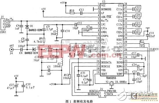
When BUSMODE=0, the bus mode of TDA5255 is I2C. The microcontroller sets the operating mode of the TDA5255 via the I2C bus. BUSCLK and BUSDATA are the bus clock line and the bus data line, respectively.
When the Rx/Tx pin is left floating or high, the TDA5255 is in the transmit state. At this time, the RF signal is transmitted from the antenna via C6, C8, C9, L1, C11 to the low noise amplifier input pin. R9 is high impedance and does not affect circuit matching. C6 is a DC decoupling capacitor. The other input signal of the differential low noise amplifier can be AC ​​coupled through a large capacitor. The differential low noise amplifier is now a single-ended low noise amplifier that is easier to match. Important matching components are C8, C9, L1 and C11.
The Rx/Tx pin is grounded or programmed to put the device in a receive state. At this time, the Rx/Tx pin operates in an open-drain state, the output logic is low, and the RF is low-resistance. The DC current flows from VCC via L2, L3, D2, R9 and D1 to GND. Because R9 has high resistance, C6, C4, and C5 have large capacitance values. The circuit simplifies the RF signal. At this point the low noise amplifier RF is grounded, so the low noise amplifier input has no power consumption. Power amplifier matching depends mainly on C8, C28, L2, C29 and L3. It should be noted that C8 cannot be modified when designing the amplifier to match, because its value has been determined by the low noise amplification input match. To accurately calculate the external capacitance, the capacitance on the pad and the parasitic capacitance between the pin and the switch (C20, C22, C23) must be considered.
The PWD/DD pin is used to set the high and low power modes of the RF device. The DATA pin is a data pin. In the transmit mode, the MCU sends a signal to the RF device. In the receive mode, if the signal can be received, the pin has the same waveform as the transmitter, and the test delay is 25μs. When the signal is not received, this pin outputs irregular pulse clutter. In actual use, you can remove the clutter by modifying the RSSI signal threshold of the TDA5255 so that the DATA pin remains low when no valid information is received.
3 Microcontroller and software design3.1 Introduction to XC866 Microcontroller
The microcontroller uses Infineon's XC866 8-bit microcontroller. The XC866 is based on the XC800 core, which is compatible with the standard 8051 processor. The XC866 has an integrated oscillator or embedded voltage regulator (can be powered from a single 3.3 V or 5.0 V supply).
The XC866's Synchronous Serial Channel (SSC) supports full-duplex and half-duplex synchronous communications. Data is transmitted and received over the TXD and RXD lines, which are typically connected to pins MTSR (Master Transmit/Slave Receive) and MRST (Master Receive/Slave Transmit). The clock signal is output by MS_CLK (Master Serial Shift Clock) or from SS_CLK (Slave Serial Shift Clock), which are typically connected to pin SCLK. Both the transmission and reception of data have buffer registers. The half-duplex communication method is used for information transmission between the TDA5255 and the internal register value of the TDA5255 is set by the I2C bus protocol.
The microcontroller completes the TDA5255's working mode setting, controls the TDA5255 to send valid information, and receives and processes the data received by the TDA5255. P1.0 and P1.1 are respectively connected to RXD0 and TXD0 of MAX3232 to complete serial communication with PC.
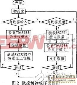
3.2 Software Design
The software program flow chart is shown in Figure 2.
Send data by first sending a "0", then send a "1", and then send the information bit "0" or "1", so after the rising edge, delay 1.5 basic time to obtain the information code. As shown in Figure 3. The definition of the basic time determines the rate at which information is sent. Take 100μs here. An information code is transmitted every 300 μs at a transmission rate of 3.3 kb/s. The TDA5255 has a maximum data rate of up to 100 kb/s.

The designed RF transceiver can transmit short-distance information, and send any information of the PC through the connection with the PC, and can also display the obtained feedback information on the host computer interface. The system is applied to the controller of the electric trolley, and the control effect is good. It can also be used as a module for transplantation, and it can be applied to close-range remote control.
Optical Fiber Patch Cord,Outdoor Ruggedized Patch Cords,Duplex Armoured Patch Cord,Indoor Patch Cord
ShenZhen JunJin Technology Co.,Ltd , https://www.jjtcl.com