First, the application background:
Magnetron sputtering is a secondary sputtering of a magnetron mode of operation. This technology is widely used in coating equipment, it is not only suitable for a wide range of coating targets (such as: copper, titanium, chrome, stainless steel, nickel and other metal materials), but also greatly enhance the film layer when coating Focus, repeatability, density and uniformity.
The magnetron sputtering coating equipment mainly uses DC magnetron sputtering, which often requires two output DC power supplies. After setting a voltage value, it is required to respond quickly to the set value of the voltage. The power supply must be stable during use and the voltage value cannot be affected by the load. However, the switching power supply commonly used in the market is open-loop control, which cannot ensure stable output, and a stable voltage is very important for the coating quality. Therefore, it is envisaged to realize the power supply by using the PID algorithm of the PLC and using the existing DC switching power supply. Quick adjustment and closed loop management.
As shown in the figure below, 4AI is needed to detect the current signal and voltage signal of the two DC stabilized power supply on the intelligent power control system as the feedback signal of the intelligent power supply; 2AO is needed to control the voltage output, so that the power supply has good load characteristics. , keep the constant voltage output.
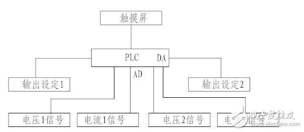
In order to meet the above requirements, PLC selects the S20M0T switch and analog hybrid host of the sea, the host comes with 4 AI analog linear inputs, 2 AO analog linear outputs, analog supports engineering quantities, AI\AQ register Can be directly accessed, very convenient in analog signal processing, saving a lot of programming time; the host also supports 32-channel PID instructions; more importantly, a host is fixed, no need to add additional expansion modules, economical.
The commonly used switching power supply in the market is open-loop control, which can not ensure stable output, and a stable voltage is very important for the coating quality. Therefore, it is envisaged to use the existing PID switching power supply to realize the power supply through the PLC PID algorithm. Quick adjustment and closed loop management.
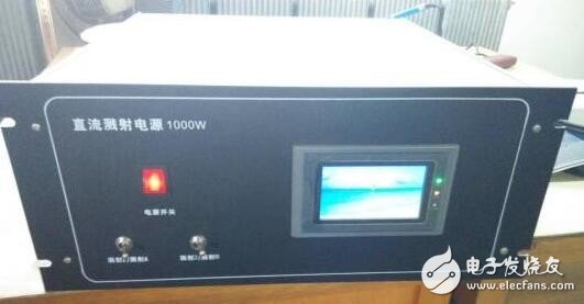
Figure 1 front view of the chassis
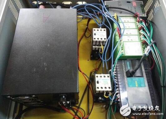
Figure 2 internal circuit
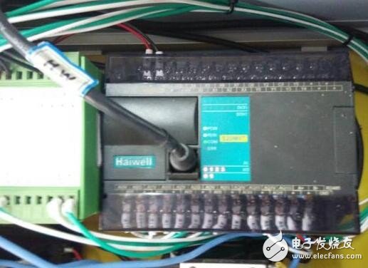
Figure 3 PLC
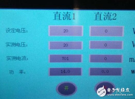
Figure 4 touch screen interface
The commonly used switching power supply in the market is open-loop control, which can not ensure stable output, and a stable voltage is very important for the coating quality. Therefore, it is envisaged to use the existing PID switching power supply to realize the power supply through the PLC PID algorithm. Quick adjustment and closed loop management.
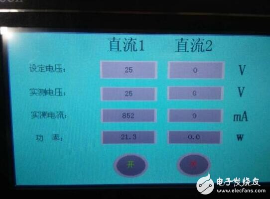
Figure 5 touch screen interface
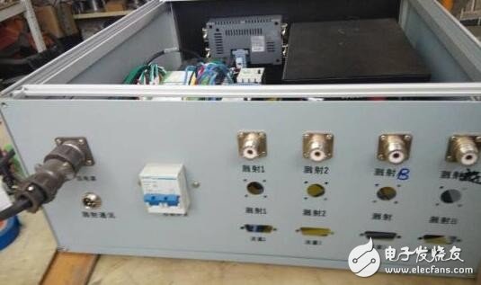
Figure 6 chassis back
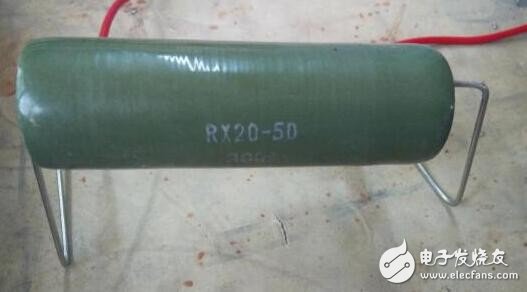
Figure 7 analog load resistance
The PID instruction, that is, the PID instruction in the special control instruction, is supported by the full range of PLCs. According to the change of load, the system adjusts the parameters in combination with the real-time curve table provided by the software during online monitoring, and adjusts the three parameters of PID one by one to achieve the best effect. After the parameters are debugged and adjusted, the voltage is quickly adjusted and stabilized, and the closed-loop management of the power supply is realized, which provides a good foundation for better magnetron sputtering coating.
The first time I used the sea as a PLC, I felt that the programming software was very user-friendly and easy to use.
[Recommended article] Water tower water level system PLC control
HDI PCB Specification
High density interconnect (HDI) PCBs represent one of the fastest-growing segments of the printed circuit board market. Because of its higher circuitry density, the HDI PCB design is able to incorporate finer lines and spaces, smaller vias and capture pads, and higher connection pad densities. A high density PCB features blind and buried vias and often contains microvias that are .006 in diameter or even less.
HDI PCBs are characterized by high-density attributes including laser microvias, fine lines and high performance thin materials. This increased density enables more functions per unit area. Higher technology HDI PCBs have multiple layers of copper filled stacked microvias (Advanced HDI PCBs) which creates a structure that enables even more complex interconnections. These very complex structures provide the necessary routing solutions for today's large pin-count chips utilized in mobile devices and other high technology products.
The HDI PCBs we offer include the following highly requested characteristics:
Blind and/or buried vias
Via-in-pad
Through vias from surface to surface
20 µm circuit geometries
30 µm dielectric layers
50 µm laser vias
125 µm bump pitch processing
Applications
HDI PCB is used to reduce size and weight, as well as to enhance electrical performance of the device. HDI PCB is the best alternative to high layer-count and expensive standard laminate or sequentially laminated boards. HDI incorporate blind and buried vias that help to save PCB real estate by allowing features and lines to be designed above or below them without making a connection. Many of today's fine pitch BGA and flip-chip component footprints do not allow for running traces between the BGA pads. Blind and buried vias will only connect layers requiring connections in that area.
HDI PCB,Special HDI PCB,HDI Prototype PCB,HDI Board PCB
Storm Circuit Technology Ltd , https://www.stormpcb.com