This scheme adopts ARM processor as the control core and constructs the design method and process of the embedded system of fingerprint recognition algorithm. The system uses optical fingerprint sensor (built-in GSK Microelectronics Co., Ltd. optical GC0307 CMOS image acquisition chip) and ARM Cortex M3 core STMicroelectronics 32-bit high-performance microcontroller STM32F205RE to form the functional body, using Sobel edge detection operator, Image acquisition and processing algorithms such as Gabor filtering and image binarization identify fingerprint images. After repeated practice, the scheme is suitable for the development of embedded components, such as biometric fingerprint feature extraction, recognition, fingerprint identity authentication, comparison and other occasions. The system is cost-effective and easy to interact, with high recognition rate and strong scalability, which is convenient for embedded applications.
0 Preface
With the increasing application of electronic information technology, many occasions require identification or identity records for specific user groups, such as access control systems, time and attendance systems, and security authentication systems. Various technologies are used in various systems, such as the retina. Identification, face recognition, fingerprint recognition, RFID radio frequency identification applications, etc. Among them, the biometric identification method has been recognized and accepted by more and more people because of its convenience and high security. Especially the fingerprint identification technology has become one of the most widely used biometric identification technologies. Therefore, the research on fingerprint recognition system based on embedded architecture has practical significance and broad application prospects.
1 system overall structure
The system uses an optical fingerprint sensor (the optical GC0307 CMOS image acquisition chip built-in from GECO Microelectronics Co., Ltd.) and the ARM Cortex M3 core STMicroelectronics 32-bit high-performance microcontroller STM32F205RE to form the functional body, using Sobel edge detection operator, Gabor Filtering, image binarization and other image acquisition and processing algorithms identify the fingerprint image, and build a small-volume embedded fingerprint recognition module. It has built-in embedded, micro-power, easy to use program interface, easy for secondary development and recognition. High accuracy, high cost performance and so on.
2 system hardware circuit design
The entire system design constitutes an integrated optical fingerprint recognition module. The module design adopts the principle of optical dark background imaging, and adds a special living body detection chip to solve the problem of residual fingerprint misidentification and rubber false fingerprint while solving the dry finger effect.
Figure 1 shows the schematic diagram of the application circuit of the optical GC0307 CMOS image acquisition chip from GECO Microelectronics Co., Ltd. This CMOS image acquisition chip is a built-in component of a high-precision, low-power, micro-volume, high-performance camera that combines CMOS image sensors for high-quality VGA images with highly integrated image processors, embedded power supplies, and high-quality The lens group is combined to output a JPEG image or image video stream, supports 8/10 digit digital transmission of JPEG images and YCbCr interface, providing a complete imaging solution.
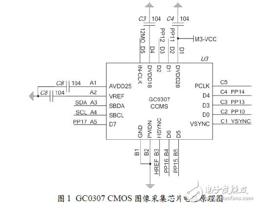
The CMOS image acquisition core function output serial data pin, clock signal pin, reset pin, serial bus pin, etc. are all connected to the GPIO port of the STM32F205RE, and the image information acquired by the CMOS chip is read through the GPIO port analog timing. . Since the STM32F205RE's GPIO port can operate at 120 MHz, the timing can be simulated very accurately and efficiently. The original image of the measured 640 & TImes; 480 can be acquired into the main processor STM32F205RE for image processing at 10 frames/s.
3 system software function design
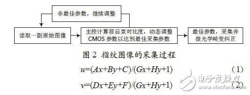
The fingerprint image acquisition process of this system is shown in Figure 2. The system software design part uses a four-point correction algorithm for distortion correction.
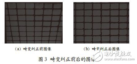
The transformation from (x, y) to (u, v) can be obtained by formula (1) and formula (2), where A ~ H is determined by the optical path, which can be finally determined by specific measurement data, and the raw data can be obtained through actual measurement. . Figure 3 shows the difference in effect between the original image and the image before and after the distortion correction. Through the transformation, the distortion corrected image can be transformed to a resolution of 500 DPI, which lays a foundation for subsequent high-quality image processing data.
ZOOKE provides you with safe and reliable connector products, with 1.25 spacing products providing more possibilities for limited space and creating more value for the research and development and production of terminal products.
1.25 wire to board connectors,1.25 connectors,ZOOKE connectors
Zooke Connectors Co., Ltd. , https://www.zooke.com