Traditional smart cars, especially embedded systems, are generally embedded systems based on single-chip or ARM. They are basically composed of software systems and hardware systems. The hardware system is the same as the traditional hardware environment. Tailoring and function expansion, however, the project's topic is to build an embedded hardware environment through xilinx's FPGA development board. From the minimum system to the IP core, it is expanded according to needs, achieving one-to-one expansion. Waste of resources, and the biggest advantage of FPGA-based embedded systems is that there are both parallel execution efficiency of PFGA and logical process analysis control of embedded software.
Overall design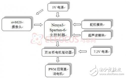
Figure 1 system hardware block diagram
Using Spartan-6's XC6SLX16 CSQ234 as the main controller, the sensor uses the camera ov6620 image acquisition module (both path) and uses the ultrasonic module (HCSR04) to measure the distance. Because of the complementary characteristics of the two, it can control the operation of the car very well. State, using the fuzzy algorithm to calculate the required speed of the motor, and the steering angle of the steering gear, thus achieving a steadily gradual.
1 main controller selectionSolution: Use a programmable logic device FPGA as the controller. FPGA can realize complex logic functions, large scale, high density, small size, high stability, rich IO resources, easy to extend peripheral functions, and the cost of FPGAs is gradually reduced, and the construction of FPGA-based embedded systems has become feasible. Both traditional embedded software flexibility and FPGA fast parallel execution efficiency.
In summary, we chose Nexys3 Spartan-6 as the main controller of the system.
2 power regulator chip selectionIn this system, the Spartan-6 main controller.
Solution: Due to the high power consumption of the DC motor, it is decided to use 7.2V, 2000mAh battery as the power supply. The LM25xx series monolithic integrated switching power supply is used as the buck chip, which can provide high-power output with high conversion efficiency and stable performance.
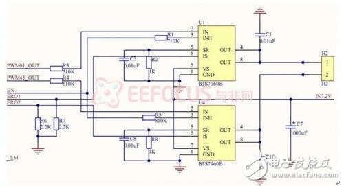
3 motor drive selectionSolution: The BTS7960B is used to build a full-bridge driver, which can meet the high-power output and drive two motors separately.
Camera module selection
Solution: The digital camera ov6620 is adopted, the control is simple, the price is suitable, and the signal is stable.
System hardware design 1 car body modelThe physical object is shown below.
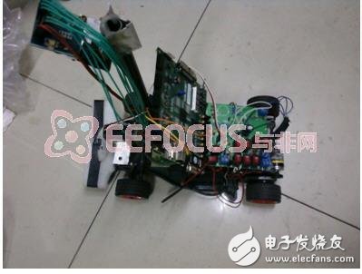
Figure 2 actual model of the car body
The camera looks for black lines, guides the car to track, ultrasonic ranging, and guides the car to control the speed.
2 power supplyThe schematic diagram is shown in Figure 3:
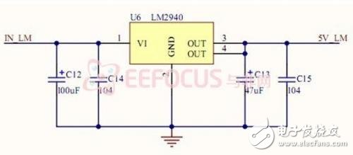
7.2V input, stable output 5V
3Ov6620 camera sensor moduleOV6620 timing analysis
The timing of the synchronization signal of the OV6620 is as follows: The field sync signal VSYN is the timing of scanning one frame between two positive pulses, that is,
A complete frame of image is between two positive pulses; the line sync signal HREF scans the timing of each row of pixels in the frame image,
That is, the high level is the effective time for scanning a row of pixels; the pixel synchronization signal PCLK provides a synchronization signal for reading the effective pixel value.
No. When the level is high, valid image data is output. The following figure shows the three synchronization signals of OV6620 VSYN, HREF and PCLK.
Timing relationship between:
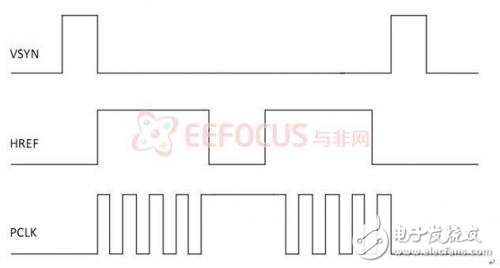
VYNSC is to determine whether an image starts, the period is 20ms, and the high level duration is very short; HREF is the judgment
Whether the break is the beginning of a line of images, the period is about 63us, and the high level duration is 40US, the low level continues
Time 23US, then we can calculate the resolution of OV6620 with reference to the timing chart: 20ms/63us=317,
Of course, there isn't that much, there are only 292 lines after the blanking and invalid signals are removed; the effective grayscale data is in the line.
It is within the rising edge after the break, so do not collect after the 23US after the line break. Calculate how many OV6620 a line
Less points: 40us/110ns=363, there are only 356 points after the blanking and invalid signals are removed. Sufficient to prove
The resolution of the OV6620 is 356*292. Observed by the oscilloscope, the period of PCLK is only 150ns, according to the single chip.
The bus of the machine can't capture this signal at all. At this time, the waveform of PCLK has become a sharp wave, and it has no meaning to capture.
This signal is taken as soon as possible when the image is acquired.
4 DC motor driveThe BTS7960B is used in the system to build a full-bridge drive, which can meet the high-power output and drive two motors separately.
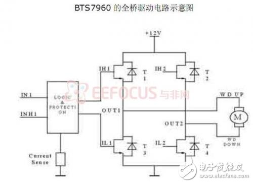
The chip inside the BTS7960B is a half bridge. The INH pin is high to enable the BTS7960. The IN pin is used to determine which MOSFET is turned on. When IN=1 and INH=1, the high-side MOSFET turns on and the OUT pin outputs a high level; when IN=0 and INH=1, the low-side MOSFET turns on and the OUT pin outputs a low level. The size of the external resistor of the SR pin can adjust the time when the MOS transistor is turned on and off, and has the function of preventing electromagnetic interference.
3.5 The figure below is the smallest embedded system built by FPGA, which is built according to the official EDK requirements of xilinx.
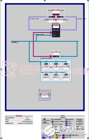
The software design is mainly divided into three parts, the first part is the construction of the minimum system (software initialization), the second part is the drive of the external hardware, and the third part is the core algorithm.
1 minimum system setup (software initialization):
Use the EDK tools to build the smallest embedded system.
2 external hardware drivers:
The external hardware driver chooses to add to the minimum system in the form of an IP core. The driver core code is written in the hardware description language, and then the software drives the external hardware through the register.
3 core algorithms:
This part is the core of the whole system, and its structural block diagram is shown below:
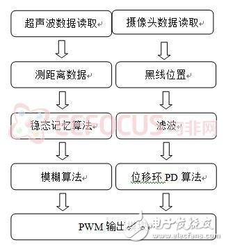
Figure 10 software structure block diagram
5 system debugging and testingCommissioning process:
5.1 hardware platform solution test
In the EDK design, you can create a new test code, automatically generate test code, and print the verification results through the serial port.
5.2 Use of ultrasonic modules
In the process of adding an IP core, it is necessary to describe the driving process in a hardware description language according to the timing requirements of the ultrasonic wave.
Process(Bus2IP_Clk,slv_reg1,the_end)
Begin
If slv_reg1=x"00000000" then
Counter<=x"00000000";
Chao_out <= '0';
Div_clk<='0';
Elsif rising_edge(Bus2IP_Clk) then
If the_end <= '1' then
Chao_out <= '1';
Counter<=counter+1;
If(counter=x"1F4") then
Counter<=x"00000000";
Chao_out <= '0';
Div_clk<='1';
End if;
End if;
End if;
End process;
-- implement slave model software accessible register(s) read mux
SLAVE_REG_READ_PROC : process( Bus2IP_Resetn, slv_reg_read_sel, slv_reg0, slv_reg1, Bus2IP_Clk, div_clk ) is
Begin
Case slv_reg_read_sel is
When "10" =>
If Bus2IP_Resetn = '0' then
TImer_count <= x"00000000";
The_end <= '0';
Elsif div_clk='1' then
If slv_chao_in='1' then
The_end <= '0';
TImer_count <= TImer_count + 1;
Else
Slv_ip2bus_data <= TImer_count; --slv_reg0;
The_end <= '1';
Timer_count <= x"00000000";
End if;
Else
Slv_ip2bus_data <= slv_reg0;
End if;
When "01" => slv_ip2bus_data <= slv_reg1;
When others => slv_ip2bus_data <= (others => '0');
End case;
End process SLAVE_REG_READ_PROC;
5.3 Debugging of PWM Module
Since two PWMs are required to operate the servo and DC motor separately, all PWM debugging is critical.
code show as below:
Intmain()
{
Unsignedlongi,j;
//close PWM
PWM_IP_mWriteSlaveReg1(XPAR_PWM_IP_0_BASEADDR,0,0x00); //PWM0
PWM_IP_mWriteSlaveReg1(XPAR_PWM_IP_1_BASEADDR,0,0x00); //PWM1
For(i=0;i<=99999;i++);
PWM_deal(0x2E);
While(1)
{
PWM_deal(0x2E);
Delay(60);
PWM_deal(0x38);
Delay(60);
PWM_deal(0x2E);
Delay(60);
PWM_deal(0x24);
Delay(60);
}
Return0;
}
voidPWM_deal(unsignedcharreg0)
{
//PWM0 steering gear
//PWM frequency
PWM_IP_mWriteSlaveReg1(XPAR_PWM_IP_0_BASEADDR,0,0x1F4);
//PWM duty cycle
PWM_IP_mWriteSlaveReg0(XPAR_PWM_IP_0_BASEADDR,0,reg0);
//PWM1 DC motor
PWM_IP_mWriteSlaveReg1(XPAR_PWM_IP_1_BASEADDR,0,0x1F4); //
PWM_IP_mWriteSlaveReg0(XPAR_PWM_IP_1_BASEADDR,0,reg0); //slv_reg0
The lcd projector is the product of the combination of liquid crystal display technology and projection technology. It uses the electro-optic effect of liquid crystal to control the transmittance and reflectivity of the liquid crystal unit through the circuit, thereby producing different gray levels and as many as 1670 million colors. Beautiful image. The main imaging device of LCD projector is liquid crystal panel. Led projector, generally refers to the light source of the projector is LED light source, the brightness is not high, within 500 lumens. The difference between dlp and led, most of them are in Projection field to distinguish.
lcd home projector,led lcd home projector,best home lcd projector,lcd home theatre projectors,best lcd home theater projector
Shenzhen Happybate Trading Co.,LTD , https://www.szhappybateprojectors.com